This thread has been locked.

If you have a related question, please click the "Ask a related question" button in the top right corner. The newly created question will be automatically linked to this question.

TMS320F28075: SDFM: PWMSYNC is resetting the SDDATA Registers

Part Number: TMS320F28075
Other Parts Discussed in Thread: AMC1303E2510

Hi,

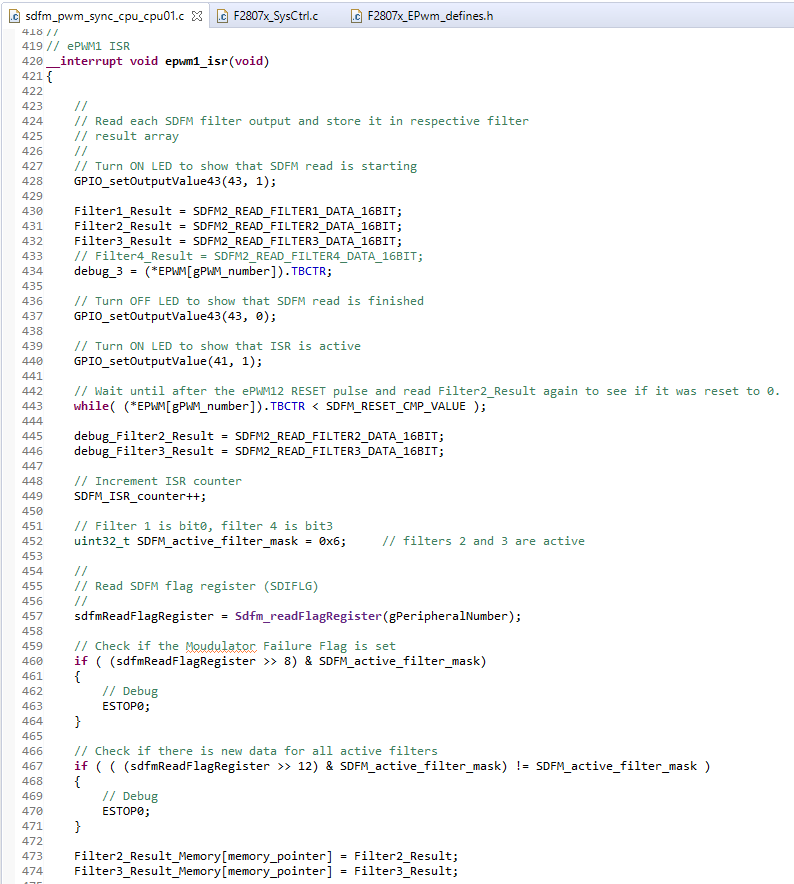
I'm using Filters 2 and 3 of the TMS320F28075 SDFM to read the Manchester Encoded output from 2 separate AMC1303E2510 chips. The AMC1303E2510 has it's own internally generated 10MHz CLK, therefore I'm using CMPC and CMPD of ePWM12 to synchronise filters 2 and 3 of SDFM2.

In section 12.1.2 of the document "Texas TMS320F2807x Tech Ref spruhm9b" it states "The FILRES input does not reset the data registers in the Filter Unit". However during testing I've found that ePWM12.CMPC and CMPD set the SDDATA registers to 0.

In my code I have an interrupt to read the SDFM SDDATA registers.

- At the beginning of the interrupt the SDFM data registers are read, they are some non-zero value.

- Then the interrupt waits until the ePWM counter has passed CMPC and CMPD.

- Then it reads the SDFM SDDATA registers again, now they have been set to 0.

So I'm just wondering if you can confirm what the behaviour of the SDDATA register is when ePWM12.CMPC and CMPD are used to reset the filters. Does SDDATA get reset to 0?

Thanks,

Fearghal

  • Fearghal,

    Can you please provide me the setup on how you saw this behavior? How are you timing your SDFM data register reads with respect to PWM sync?

    Regards,
    Manoj
  • Hi Manoj,

    I've attached the main .c file of the project. Below I've also pasted the relevant piece of code for the ISR that reads the SDFM registers.

    epwm1_isr is triggered when ePWM1 counter is 0. It is configured in UP COUNT mode. The PWM period is set to 4 times the SDFM sampling period. This is because after a PWM sync, the first two SDFM output values are incorrect (with a SINC3 filter). ePWM12 is setup the same as ePWM1 and is synced to the ePWM1 counter by the synchronisation pulse input from ePWM1 fed through ePWM10 and 11.

    ePWM12.CMPC and CMPD are set to SDFM_RESET_CMP_VALUE. SDFM_RESET_CMP_VALUE is set so that it occurs Latency of data filter + 5 SD clock cycles before the PWM counter resets to 0. Therefore after the CMPC/CMPD PWM sync there should be time for 3 SDFM output values before the ISR triggers.

    When the ISR triggers, the SDFM DATA registers are read straight away (lines 431 - 432 below) and saved in "Filter2_Result" and "Filter3_Result". (Note that although Filter 1 is read too, there isn't actually any input to filter 1. Only filters 2 and 3 have input data streams).

    Next the ISR waits until the PWM count is > SDFM_RESET_CMP_VALUE (i.e until after the ePWM12.CMPC/CMPD PWM sync), line 443.

    Then the SDFM DATA registers are read again and the results are saved in "debug_Filter2_Result" and "debug_Filter3_Result".

    I can watch the values "Filter2_Result", "Filter3_Result", "debug_Filter2_Result" and "debug_Filter3_Result" in the Code Composer debug window while the code is running. Here I can see that "Filter2_Result" and "Filter3_Result" are always as expected (i.e. some non-zero value) but "debug_Filter2_Result" and "debug_Filter3_Result" are always equal to zero. Therefore I'm concluding that the ePWM12.CMPC/CMPD sync pulse is resetting the SDDATA registers 0. Does that make sense? Or am I missing something?

    sdfm_pwm_sync_cpu_cpu01.c
    //###########################################################################
    //
    // FILE:   sdfm_pwm_sync_cpu_cpu01.c
    //
    // TITLE:  SDFM PWM sync Example for F2807x.
    //
    //! \addtogroup cpu01_example_list
    //! <h1> SDFM PWM Sync </h1>
    //!
    //! In this example, SDFM filter data is read by CPU in SDFM ISR routine. The
    //! SDFM configuration is shown below:
    //!     - SDFM1 is used in this example
    //!     - MODE0 Input control mode selected
    //!     - Comparator settings
    //!         - Sinc3 filter selected
    //!         - OSR = 32
    //!         - HLT = 0x7FFF (Higher threshold setting)
    //!         - LLT  = 0x0000(Lower threshold setting)
    //!  -  Data filter settings
    //!      - All the 4 filter modules enabled
    //!      - Sinc3 filter selected
    //!      - OSR = 256
    //!      - All the 4 filters are synchronized by using PWM
    //!      - Filter output represented in 16 bit format
    //!      - In order to convert 25 bit Data filter
    //!        into 16 bit format user needs to right shift by 9 bits for
    //!        Sinc3 filter with OSR = 256
    //!  - Interrupt module settings for SDFM filter
    //!      - All the 4 higher threshold comparator interrupts disabled
    //!      - All the 4 lower threshold comparator interrupts disabled
    //!      - All the 4 modulator failure interrupts disabled
    //!      - All the 4 filter will generate interrupt when a new filter data
    //!        is available
    //!
    //
    //###########################################################################
    // $TI Release: F2807x Support Library v3.05.00.00 $
    // $Release Date: Tue Jun 26 03:19:11 CDT 2018 $
    // $Copyright:
    // Copyright (C) 2014-2018 Texas Instruments Incorporated - http://www.ti.com/
    //
    // Redistribution and use in source and binary forms, with or without 
    // modification, are permitted provided that the following conditions 
    // are met:
    // 
    //   Redistributions of source code must retain the above copyright 
    //   notice, this list of conditions and the following disclaimer.
    // 
    //   Redistributions in binary form must reproduce the above copyright
    //   notice, this list of conditions and the following disclaimer in the 
    //   documentation and/or other materials provided with the   
    //   distribution.
    // 
    //   Neither the name of Texas Instruments Incorporated nor the names of
    //   its contributors may be used to endorse or promote products derived
    //   from this software without specific prior written permission.
    // 
    // THIS SOFTWARE IS PROVIDED BY THE COPYRIGHT HOLDERS AND CONTRIBUTORS 
    // "AS IS" AND ANY EXPRESS OR IMPLIED WARRANTIES, INCLUDING, BUT NOT 
    // LIMITED TO, THE IMPLIED WARRANTIES OF MERCHANTABILITY AND FITNESS FOR
    // A PARTICULAR PURPOSE ARE DISCLAIMED. IN NO EVENT SHALL THE COPYRIGHT 
    // OWNER OR CONTRIBUTORS BE LIABLE FOR ANY DIRECT, INDIRECT, INCIDENTAL, 
    // SPECIAL, EXEMPLARY, OR CONSEQUENTIAL DAMAGES (INCLUDING, BUT NOT 
    // LIMITED TO, PROCUREMENT OF SUBSTITUTE GOODS OR SERVICES; LOSS OF USE,
    // DATA, OR PROFITS; OR BUSINESS INTERRUPTION) HOWEVER CAUSED AND ON ANY
    // THEORY OF LIABILITY, WHETHER IN CONTRACT, STRICT LIABILITY, OR TORT 
    // (INCLUDING NEGLIGENCE OR OTHERWISE) ARISING IN ANY WAY OUT OF THE USE 
    // OF THIS SOFTWARE, EVEN IF ADVISED OF THE POSSIBILITY OF SUCH DAMAGE.
    // $
    //###########################################################################
    
    //
    // Included Files
    //
    #include "F28x_Project.h"
    #include "F2807x_struct.h"
    #include "F2807x_sdfm_drivers.h"
    
    /* Device Related Defines */
    // TODO: confirm these numbers
    #define CPU_SYS_CLOCK (100*1000000)
    #define PWMSYSCLOCK_FREQ (50*1000000)
    #define ECAPSYSCLOCK_FREQ   (100*1000000)
    
    //
    // User Defines
    //
    #define SDFM_MODE                   MODE_2
    #define SDFM_FILTER_TYPE            SINC3
    #define SDFM_OSR                    OSR_16          // Value is for OSR_50 is actually 49
    //#define SDFM_NUM_BITS_RIGHT_SHIFT   SHIFT_2_BITS    // This setting depends on the OSR and filter type. See datasheet for details
    #define SDFM_SCALE_FACTOR           0.00001525878906 // = ( 0.5 / 32768.0 ). This assumes that the SDFM output is from -32768 to 32767 (i.e. int16_t)
    #define SDFM_NUM_BITS_RIGHT_SHIFT   SHIFT_1_BITS    // With OSR_16, use SHIFT_1_BITS to get the SDFM output in the range -2048 to 2048
    
    #if SDFM_FILTER_TYPE == SINCFAST
    #define     NUM_INCORRECT_SAMPLES_AFTER_SYNC    2
    #elif SDFM_FILTER_TYPE == SINC1
    #define     NUM_INCORRECT_SAMPLES_AFTER_SYNC    0
    #elif SDFM_FILTER_TYPE == SINC2
    #define     NUM_INCORRECT_SAMPLES_AFTER_SYNC    1
    #elif SDFM_FILTER_TYPE == SINC3
    #define     NUM_INCORRECT_SAMPLES_AFTER_SYNC    2
    #endif
    
    #define SDCLK_FREQ          ( 0.96 * 10000000.0 )        // delta-sigma device dependent if the chip uses it's own internal CLK. Use lowest possible frequency
    #define SD_OUTPUT_FREQ      ( SDCLK_FREQ / (float)(SDFM_OSR + 1) )
    #define PWM_CLK_IN_SDFM_CLK ( PWMSYSCLOCK_FREQ / SDCLK_FREQ )
    #define PWM_CLK_IN_SDFM_OSR ( PWMSYSCLOCK_FREQ / SD_OUTPUT_FREQ )
    
    // Define the filter latencies. Add 5 SD CLK cycles as per datasheet.
    // Use 0.96*SDCLK_FREQ to account for 4% tolerance on the internal CLK frequency
    // of the AMC1303
    #define SDFM2_LATENCY_PWM_CLK_COUNT     ( ( (NUM_INCORRECT_SAMPLES_AFTER_SYNC + 1) * PWM_CLK_IN_SDFM_OSR ) + ( 5.0 * PWM_CLK_IN_SDFM_CLK ) ) // ( SDFM2_LATENCY_SEC * PWMSYSCLOCK_FREQ )
    #define EPWM_TIMER_PERIOD               ( (NUM_INCORRECT_SAMPLES_AFTER_SYNC + 2) * PWM_CLK_IN_SDFM_OSR )  // ( (NUM_INCORRECT_SAMPLES_AFTER_SYNC + 2) / (1.0 * SD_OUTPUT_FREQ) ) //  (SDFM2_LATENCY_PWM_CLK_COUNT + 10)
    #define SDFM_RESET_CMP_VALUE            ( EPWM_TIMER_PERIOD - SDFM2_LATENCY_PWM_CLK_COUNT )
    
    //
    // SDFM Defines
    //
    #define SDFM_PIN_MUX_OPTION1      1
    #define SDFM_PIN_MUX_OPTION2      2
    #define SDFM_PIN_MUX_OPTION3      3
    // #define EPWM_TIMER_TBPRD          65535  // ePWM Period register
    
    //
    // DAC Defines
    //
    #define REFERENCE_VDAC              0
    #define REFERENCE_VREF              1
    #define DACA                        1
    #define DACB                        2
    #define DACC                        3
    #define DAC_REFERENCE_VOLTAGE       REFERENCE_VREF
    
    //
    // ePWM Defines
    //
    #define EPWM1_TIMER_TBPRD       EPWM_TIMER_PERIOD  // Period register
    
    #define EPWM10_TIMER_TBPRD      EPWM_TIMER_PERIOD  // Period register
    
    #define EPWM11_TIMER_TBPRD      EPWM_TIMER_PERIOD  // Period register
    #define EPWM11_CMPC             SDFM_RESET_CMP_VALUE
    #define EPWM11_CMPD             SDFM_RESET_CMP_VALUE
    
    #define EPWM12_TIMER_TBPRD      EPWM_TIMER_PERIOD  // Period register
    #define EPWM12_CMPC             SDFM_RESET_CMP_VALUE
    #define EPWM12_CMPD             SDFM_RESET_CMP_VALUE
    
    #define EPWM_CMP_UP           1
    #define EPWM_CMP_DOWN         0
    
    //
    // Globals
    //
    uint16_t gPeripheralNumber, gPWM_number = 12;
    int16_t  Filter1_Result = 0;
    int16_t  Filter2_Result = 0;
    int16_t  Filter3_Result = 0;
    int16_t  Filter4_Result = 0;
    uint16_t  SDFMReadingCounter = 0;
    uint32_t sdfmReadFlagRegister;
    
    #pragma DATA_SECTION(Filter1_Result,"Filter1_RegsFile");
    #pragma DATA_SECTION(Filter2_Result,"Filter2_RegsFile");
    #pragma DATA_SECTION(Filter3_Result,"Filter3_RegsFile");
    #pragma DATA_SECTION(Filter4_Result,"Filter4_RegsFile");
    volatile struct DAC_REGS* DAC_PTR[4] = {0x0,&DacaRegs,&DacbRegs,&DaccRegs};
    
    //
    // Function Prototypes
    //
    void Sdfm_configurePins(uint16_t);
    void InitEPwm(void);
    void done(void);
    void GPIO_configureDiagnosticPins(void);
    void GPIO_setOutputValue(uint32_t GPIONumber, uint32_t outputValue);
    void GPIO_setOutputValue43(uint32_t GPIONumber, uint32_t outputValue);
    void configureDAC(Uint16 dac_num);
    __interrupt void Sdfm2_ISR(void);
    
    void InitEPwm1Example(void);
    void InitEPwm10Example(void);
    void InitEPwm11Example(void);
    void InitEPwm12Example(void);
    __interrupt void epwm1_isr(void);
    
    // Debug variables
    #define MEMORY_SIZE     16
    uint32_t SDFM_ISR_counter = 0;
    int16_t  Filter2_Result_Memory[MEMORY_SIZE];
    int16_t  Filter3_Result_Memory[MEMORY_SIZE];
    uint16_t memory_pointer = 0;
    int32_t debug_1 = EPWM1_TIMER_TBPRD;
    int32_t debug_2 = SDFM_RESET_CMP_VALUE;
    int16_t  debug_Filter2_Result;
    int16_t  debug_Filter3_Result;
    int32_t debug_3;
    int32_t debug_4;
    int32_t debug_5;
    int32_t debug_6;
    int32_t debug_7;
    int32_t debug_8;
    int32_t debug_9;
    int32_t debug_10;
    
    //
    // Main
    //
    void main(void)
    {
       uint16_t  pinMuxoption;
       uint16_t  HLT, LLT;
    
    //
    // Initialize System Control:
    // PLL, WatchDog, enable Peripheral Clocks
    // This example function is found in the F2807x_SysCtrl.c file.
    //
        InitSysCtrl();
    
    //
    // Clear all __interrupts and initialize PIE vector table:
    // Disable CPU __interrupts
    //
        DINT;
    
    //
    // Initialize PIE control registers to their default state.
    // The default state is all PIE __interrupts disabled and flags
    // are cleared.
    // This function is found in the F2807x_PieCtrl.c file.
    //
        InitPieCtrl();
    
    //
    // Disable CPU __interrupts and clear all CPU __interrupt flags:
    //
        IER = 0x0000;
        IFR = 0x0000;
    
    //
    // Initialize the PIE vector table with pointers to the shell Interrupt
    // Service Routines (ISR).
    // This will populate the entire table, even if the __interrupt
    // is not used in this example.  This is useful for debug purposes.
    // The shell ISR routines are found in F2807x_SysCtrl.c.
    // This function is found in F2807x_SysCtrl.c.
    //
        InitPieVectTable();
    
    //
    // Interrupts that are used in this example are re-mapped to
    // ISR functions found within this file.
    //
        EALLOW;
        PieVectTable.EPWM1_INT = &epwm1_isr;
        PieVectTable.SD2_INT = &Sdfm2_ISR;
        EDIS;
    
        //
        // For this example, only initialize the ePWM
        //
        EALLOW;
        CpuSysRegs.PCLKCR0.bit.TBCLKSYNC = 0;
        EDIS;
    
        InitEPwm1Example();
        InitEPwm10Example();
        InitEPwm11Example();
        InitEPwm12Example();
    
        EALLOW;
        CpuSysRegs.PCLKCR0.bit.TBCLKSYNC = 1;
        EDIS;


    //
    // Configure DACA and DACB
    //
        configureDAC(DACA);
        configureDAC(DACB);
    
    
    #ifdef CPU1
        pinMuxoption = SDFM_PIN_MUX_OPTION2;
    //
    // Configure GPIO pins as SDFM pins
    //
        Sdfm_configurePins(pinMuxoption);
    #endif
    
    //
    // Select SDFM2
    //
        gPeripheralNumber = SDFM2;
    
    //
    // Input Control Module
    //
    // Configure Input Control Mode: Modulator Clock rate = Modulator data rate
    //
        Sdfm_configureInputCtrl(gPeripheralNumber, FILTER1, SDFM_MODE);
        Sdfm_configureInputCtrl(gPeripheralNumber, FILTER2, SDFM_MODE);
        Sdfm_configureInputCtrl(gPeripheralNumber, FILTER3, SDFM_MODE);
        Sdfm_configureInputCtrl(gPeripheralNumber, FILTER4, SDFM_MODE);
    
    //
    // Comparator Module
    //
        HLT = 0x7FFF;    //Over value threshold settings
        LLT = 0x0000;    //Under value threshold settings
    
    //
    // Configure Comparator module's comparator filter type and comparator's OSR
    // value, higher threshold, lower threshold
    //
        Sdfm_configureComparator(gPeripheralNumber, FILTER1, SINC3, OSR_32,
                                 HLT, LLT);
        Sdfm_configureComparator(gPeripheralNumber, FILTER2, SINC3, OSR_32,
                                 HLT, LLT);
        Sdfm_configureComparator(gPeripheralNumber, FILTER3, SINC3, OSR_32,
                                 HLT, LLT);
        Sdfm_configureComparator(gPeripheralNumber, FILTER4, SINC3, OSR_32,
                                 HLT, LLT);
    
    //
    // Enable Master filter bit: Unless this bit is set none of the filter modules
    // can be enabled. All the filter modules are synchronized when master filter
    // bit is enabled after individual filter modules are enabled. All the filter
    // modules are asynchronized when master filter bit is enabled before
    // individual filter modules are enabled.
    //
        Sdfm_enableMFE(gPeripheralNumber);
    
    //
    // Data filter Module
    //
    // Configure Data filter modules filter type, OSR value and
    // enable / disable data filter
    // If the OSR/Filter type combination have an output range that is 16-bit or less,
    // then there is no need to right shift bits. However be careful with this.
    // Data is 25-bit by default. Right shift by 13-bits to make it 12-bit
    // Right shift by 1-bit more than needed so we don't have to multiply by 0.5 in the ISR to scale to the DAC range
        Sdfm_configureData_filter(gPeripheralNumber, FILTER1, FILTER_ENABLE, SDFM_FILTER_TYPE,
                                  SDFM_OSR, DATA_16_BIT, SDFM_NUM_BITS_RIGHT_SHIFT);
        Sdfm_configureData_filter(gPeripheralNumber, FILTER2, FILTER_ENABLE, SDFM_FILTER_TYPE,
                                  SDFM_OSR, DATA_16_BIT, SDFM_NUM_BITS_RIGHT_SHIFT);
        Sdfm_configureData_filter(gPeripheralNumber, FILTER3, FILTER_ENABLE, SDFM_FILTER_TYPE,
                                  SDFM_OSR, DATA_16_BIT, SDFM_NUM_BITS_RIGHT_SHIFT);
        Sdfm_configureData_filter(gPeripheralNumber, FILTER4, FILTER_ENABLE, SDFM_FILTER_TYPE,
                                  SDFM_OSR, DATA_16_BIT, SDFM_NUM_BITS_RIGHT_SHIFT);
    
    //
    // PWM11.CMPC, PWM11.CMPD, PWM12.CMPC and PWM12.CMPD signals cannot synchronize
    // the filters. This option is not being used in this example.
    // EDIT: they can synchronise the filters and are being used
    
        Sdfm_configureExternalreset(gPeripheralNumber,FILTER_1_EXT_RESET_ENABLE,
                                    FILTER_2_EXT_RESET_ENABLE,
                                    FILTER_3_EXT_RESET_ENABLE,
                                    FILTER_4_EXT_RESET_ENABLE);
    
    //
    // Enable interrupts
    //
    // Following SDFM interrupts can be enabled / disabled using this function.
    //  Enable / disable comparator high threshold
    //  Enable / disable comparator low threshold
    //  Enable / disable modulator clock failure
    //  Enable / disable filter acknowledge
    //
        Sdfm_configureInterrupt(gPeripheralNumber, FILTER1, IEH_DISABLE,
                                IEL_DISABLE, MFIE_DISABLE, AE_DISABLE);
        Sdfm_configureInterrupt(gPeripheralNumber, FILTER2, IEH_DISABLE,
                                IEL_DISABLE, MFIE_ENABLE, AE_ENABLE);
        Sdfm_configureInterrupt(gPeripheralNumber, FILTER3, IEH_DISABLE,
                                IEL_DISABLE, MFIE_ENABLE, AE_ENABLE);
        Sdfm_configureInterrupt(gPeripheralNumber, FILTER4, IEH_DISABLE,
                                IEL_DISABLE, MFIE_DISABLE, AE_DISABLE);
    
        // Setup Diagnostic GPIO output pins
        GPIO_configureDiagnosticPins();
    
    //
    // Enable SDFM master interrupt
    //
        Sdfm_enableMIE(gPeripheralNumber);
    
        // The interrupt triggers on counter = 0. Wait until just after we've passed zero and then
        // enable the ePWM interrupt. By doing this there should be a valid SDFM output value waiting
        // for the first interrupt
        while( ( (*EPWM[gPWM_number]).TBCTR < 10 ) || ( (*EPWM[gPWM_number]).TBCTR > 100 ) );
    
        //
        // Enable CPU INT3 which is connected to ePWM INT
        //
        IER |= M_INT3;
    
        //
        // Enable EPWM INTn in the PIE: Group 3 interrupt 1-3
        //
        PieCtrlRegs.PIEIER3.bit.INTx1 = 1;
        // Enable ePWM Interrupt
        EALLOW;
        EPwm1Regs.ETSEL.bit.INTEN = 1;                // Enable INT
        EDIS;
    
        // Enable global interrupt bit
        EINT;
    
        while(1);
    }


    //
    // ePWM1 ISR
    __interrupt void epwm1_isr(void)
    {
    
        //
        // Read each SDFM filter output and store it in respective filter
        // result array
        //
        // Turn ON LED to show that SDFM read is starting
        GPIO_setOutputValue43(43, 1);
    
        Filter1_Result = SDFM2_READ_FILTER1_DATA_16BIT;
        Filter2_Result = SDFM2_READ_FILTER2_DATA_16BIT;
        Filter3_Result = SDFM2_READ_FILTER3_DATA_16BIT;
        // Filter4_Result = SDFM2_READ_FILTER4_DATA_16BIT;
        debug_3 = (*EPWM[gPWM_number]).TBCTR;
    
        // Turn OFF LED to show that SDFM read is finished
        GPIO_setOutputValue43(43, 0);
    
        // Turn ON LED to show that ISR is active
        GPIO_setOutputValue(41, 1);
    
        // Wait until after the ePWM12 RESET pulse and read Filter2_Result again to see if it was reset to 0.
        while( (*EPWM[gPWM_number]).TBCTR < SDFM_RESET_CMP_VALUE );
    
        debug_Filter2_Result = SDFM2_READ_FILTER2_DATA_16BIT;
        debug_Filter3_Result = SDFM2_READ_FILTER3_DATA_16BIT;
    
        // Increment ISR counter
        SDFM_ISR_counter++;
    
        // Filter 1 is bit0, filter 4 is bit3
        uint32_t SDFM_active_filter_mask = 0x6;     // filters 2 and 3 are active
    
        //
        // Read SDFM flag register (SDIFLG)
        //
        sdfmReadFlagRegister = Sdfm_readFlagRegister(gPeripheralNumber);
    
        // Check if the Moudulator Failure Flag is set
        if ( (sdfmReadFlagRegister >> 8) & SDFM_active_filter_mask)
        {
            // Debug
            ESTOP0;
        }
    
        // Check if there is new data for all active filters
        if ( ( (sdfmReadFlagRegister >> 12) & SDFM_active_filter_mask) != SDFM_active_filter_mask )
        {
            // Debug
            ESTOP0;
        }
    
        Filter2_Result_Memory[memory_pointer] = Filter2_Result;
        Filter3_Result_Memory[memory_pointer] = Filter3_Result;
    
        if(memory_pointer >= (MEMORY_SIZE - 1))
        {
            memory_pointer = 0;
        }
        else
        {
            memory_pointer++;
        }
    
    
        // Debug
        if( (Filter2_Result < 1000 || Filter3_Result < 1000) &&  SDFM_ISR_counter > 0)
        {
            ESTOP0;
        }
    
    
        //
        // Write the current SDFM value to buffered DAC
        //
        // Method 1: Use this method only if the SDFM data is set to be in the range -2048 to 2048
        // TODO: it is possible that the value below could equal 4096. Need to check that writing 4096 to
        // the DAC doesn't produce unexpected results. Remember 4095 is the max DAC value.
        DAC_PTR[DACA]->DACVALS.all = Filter2_Result + 2048;
        DAC_PTR[DACB]->DACVALS.all = Filter3_Result + 2048;
    
        // Method 2: Use this method if the SDFM data is not set to be in the range -2048 to 2048
        //DAC_PTR[DACA]->DACVALS.all = ((Filter2_Result*SDFM_SCALE_FACTOR) + 0.5)*4095;
        //DAC_PTR[DACB]->DACVALS.all = ((Filter3_Result*SDFM_SCALE_FACTOR) + 0.5)*4095;
    
        //
        // Clear SDFM flag register
        //
        Sdfm_clearFlagRegister(gPeripheralNumber, sdfmReadFlagRegister);
    
        //
        // Clear INT flag for this timer
        //
        EPwm1Regs.ETCLR.bit.INT = 1;
    
        //
        // Acknowledge this interrupt to receive more interrupts from group 3
        //
        PieCtrlRegs.PIEACK.all = PIEACK_GROUP3;
    
        // Turn OFF LED to show that ISR is finished
        GPIO_setOutputValue(41, 0);
    }
    
    //
    // Sdfm2_ISR - SDFM 2 ISR
    //
    __interrupt void Sdfm2_ISR(void)
    {
        // Turn ON LED to show that ISR is active
        GPIO_setOutputValue(41, 1);
    
        // Increment ISR counter
        SDFM_ISR_counter++;
    
        uint32_t SDFM_active_filter_mask = 0x6;
    
        // Check if this interrupt was triggered by a Moudulator Failure Flag
        if ( (Sdfm_readFlagRegister(gPeripheralNumber) >> 8) & SDFM_active_filter_mask)
        {
            // Debug
            ESTOP0;
        }
    
        // Filters 2 and 3 are active. Wait until there is new data available for both.
        // Use mask to select which filters to wait for.
    
        while ( ( (Sdfm_readFlagRegister(gPeripheralNumber) >> 12) & SDFM_active_filter_mask) != SDFM_active_filter_mask )
        {
            // just wait
            // ESTOP0;
        }
    
        // We need to ignore the first few filter output values after a sync.
        SDFMReadingCounter++;
    
        //
        // Read each SDFM filter output and store it in respective filter
        // result array
        //
        Filter1_Result = SDFM2_READ_FILTER1_DATA_16BIT;
        Filter2_Result = SDFM2_READ_FILTER2_DATA_16BIT;
        Filter3_Result = SDFM2_READ_FILTER3_DATA_16BIT;
        Filter4_Result = SDFM2_READ_FILTER4_DATA_16BIT;
    
        Filter2_Result_Memory[memory_pointer] = Filter2_Result;
        Filter3_Result_Memory[memory_pointer] = Filter3_Result;
    
        if(memory_pointer >= (MEMORY_SIZE - 1))
        {
            memory_pointer = 0;
        }
        else
        {
            memory_pointer++;
        }
    
        // Debug
        if( (Filter2_Result < 8000 || Filter3_Result < 8000) &&  SDFMReadingCounter > 3)
        {
            ESTOP0;
        }
    
    
        if (SDFMReadingCounter > (NUM_INCORRECT_SAMPLES_AFTER_SYNC + 1))
        {
    
    
            SDFMReadingCounter = 0;
    
            //
            // Write the current SDFM value to buffered DAC
            //
            // TODO: it is possible that the value below could equal 4096. Need to check that writing 4096 to
            // the DAC doesn't produce unexpected results. Remember 4095 is the max DAC value.
            // DAC_PTR[DACA]->DACVALS.all = Filter2_Result + 2048;
            // DAC_PTR[DACB]->DACVALS.all = Filter3_Result + 2048;
    
            // Method 2: Use this method if the SDFM data is not set to be in the range -2048 to 2048
            DAC_PTR[DACA]->DACVALS.all = ((Filter2_Result*SDFM_SCALE_FACTOR) + 0.5)*4095;
            DAC_PTR[DACB]->DACVALS.all = ((Filter3_Result*SDFM_SCALE_FACTOR) + 0.5)*4095;
    
    
            // Reset the filter module to synchronise all 4 channels
            // Turn RESET LED ON/OFF to show sync point
            GPIO_setOutputValue43(43, 1);
            Sdfm_disableMFE(gPeripheralNumber);
            Sdfm_enableMFE(gPeripheralNumber);
            GPIO_setOutputValue43(43, 0);
    
    
        }
    
        //
        // Read SDFM flag register (SDIFLG)
        //
        sdfmReadFlagRegister = Sdfm_readFlagRegister(gPeripheralNumber);
    
        //
        // Clear SDFM flag register
        //
        Sdfm_clearFlagRegister(gPeripheralNumber, sdfmReadFlagRegister);
        // sdfmReadFlagRegister = Sdfm_readFlagRegister(gPeripheralNumber);
    
        /*
         if (sdfmReadFlagRegister != 0x0)
         {
         ESTOP0;
         }
         */
    
        //
        // Acknowledge this __interrupt to receive more __interrupts from group 5
        //
        PieCtrlRegs.PIEACK.all = PIEACK_GROUP5;
    
        // Turn OFF LED to show that ISR is finished
        GPIO_setOutputValue(41, 0);
    
    }
    
    //
    // Sdfm_configurePins - Configure SDFM GPIOs
    //
    void Sdfm_configurePins(uint16_t sdfmPinOption)
    {
        uint16_t pin;
        uint16_t flagMask;
    
        flagMask = GPIO_ASYNC;
    
        // Need to invert the SDFM data pins if data is Manchester encoded. This is because the delta-sigma chips use IEEE 802.3 Manchester standard
        // but this micro uses G.E. Thomas Manchester standard
    #if SDFM_MODE == MODE_2
    
        flagMask |= GPIO_INVERT;
    
    #endif
    
        switch (sdfmPinOption)
        {
            case SDFM_PIN_MUX_OPTION1:
                for(pin=16;pin<=31;pin++)
                {
                    GPIO_SetupPinOptions(pin, GPIO_INPUT, flagMask);
                    GPIO_SetupPinMux(pin,GPIO_MUX_CPU1,7);
                }
                break;
    
            case SDFM_PIN_MUX_OPTION2:
                for(pin=48;pin<=63;pin++)
                {
                    GPIO_SetupPinOptions(pin, GPIO_INPUT, flagMask);
                    GPIO_SetupPinMux(pin,GPIO_MUX_CPU1,7);
                }
                break;
    
            case SDFM_PIN_MUX_OPTION3:
                for(pin=122;pin<=137;pin++)
                {
                    GPIO_SetupPinOptions(pin, GPIO_INPUT, flagMask);
                    GPIO_SetupPinMux(pin,GPIO_MUX_CPU1,7);
                }
                break;
        }
    }
    
    //
    // InitEPwm - Initialize specified EPWM settings
    //
    void InitEPwm(void)
    {
        uint16_t CMPC,CMPD;
    
        CMPC = 200;
        CMPD = 200;
    
    #ifdef CPU1
        GPIO_SetupPinOptions(4, GPIO_OUTPUT, GPIO_ASYNC);
        GPIO_SetupPinMux(4,GPIO_MUX_CPU1,1);
    #endif
    
        EALLOW;
    
        //
        // Allows all users to globally synchronize all enabled ePWM modules to
        // the time-base clock (TBCLK)
        //
        CpuSysRegs.PCLKCR0.bit.TBCLKSYNC = 1;
    
        //
        // Setup TBCLK
        //
        (*EPWM[gPWM_number]).TBPHS.bit.TBPHS = 0x0000;    // Phase is 0
        (*EPWM[gPWM_number]).TBCTR = 0x0000;              // Clear counter
        //(*EPWM[gPWM_number]).TBPRD = EPWM_TIMER_TBPRD;    // Set timer period
                                                          // 801 TBCLKs.
    
        (*EPWM[gPWM_number]).CMPC = CMPC;                 // Set Compare C value
        (*EPWM[gPWM_number]).CMPD = CMPD;                 // Set Compare D value
    
        (*EPWM[gPWM_number]).CMPA.bit.CMPA = CMPC;        // Set Compare C value
        (*EPWM[gPWM_number]).CMPB.bit.CMPB = CMPD;        // Set Compare D value
    
        //
        // Setup counter mode
        //
        (*EPWM[gPWM_number]).TBCTL.bit.CTRMODE = TB_COUNT_UP; // Count up
        (*EPWM[gPWM_number]).TBCTL.bit.HSPCLKDIV = TB_DIV1;
        (*EPWM[gPWM_number]).TBCTL.bit.CLKDIV = TB_DIV1;
    
        //
        // Set actions
        //
        (*EPWM[gPWM_number]).AQCTLA.bit.CAU = 3;      // Set PWM1A on event A, up
                                                      // count
    
        //
        // Set actions
        //
        (*EPWM[gPWM_number]).AQCTLB.bit.CBU = 3;      // Set PWM1A on event A, up
                                                      // count
    
        EDIS;
    }
    
    // Setup Diagnostic GPIO pins
    void GPIO_configureDiagnosticPins(void)
    {
        //
           // These can be combined into single statements for improved
           // code efficiency.
           //
    
           //
           // Enable GPIOs for uP_DIAGNOSTIC0-13 (except 6 and 7) as outputs
           //
           EALLOW;
    
           // DIAGNOSTIC0. ALSO SD2_D4, NO NOT USE
           /*
           // GpioCtrlRegs.GPBPUD.bit.GPIO62 = 0;   // Enable pullup on GPIO56
           GpioDataRegs.GPBSET.bit.GPIO62 = 1;   // Load output latch
           GpioCtrlRegs.GPBMUX2.bit.GPIO62 = 0;  // GPIO56 = GPIO56
           GpioCtrlRegs.GPBDIR.bit.GPIO62 = 1;   // GPIO56 = output
           */
    
           // DIAGNOSTIC1. ALSO SD2_D3, NO NOT USE
           /*
           GpioCtrlRegs.GPBPUD.bit.GPIO60 = 0;   // Enable pullup on GPIO56
           GpioDataRegs.GPBSET.bit.GPIO60 = 1;   // Load output latch
           GpioCtrlRegs.GPBMUX2.bit.GPIO60 = 0;  // GPIO56 = GPIO56
           GpioCtrlRegs.GPBDIR.bit.GPIO60 = 1;   // GPIO56 = output
           */
    
           // DIAGNOSTIC2. ALSO SD2_C2, NO NOT USE
           /*
           GpioCtrlRegs.GPBPUD.bit.GPIO59 = 0;   // Enable pullup on GPIO56
           GpioDataRegs.GPBSET.bit.GPIO59 = 1;   // Load output latch
           GpioCtrlRegs.GPBMUX2.bit.GPIO59 = 0;  // GPIO56 = GPIO56
           GpioCtrlRegs.GPBDIR.bit.GPIO59 = 1;   // GPIO56 = output
           */
    
           // DIAGNOSTIC3. ALSO SD2_D2, NO NOT USE
           /*
           GpioCtrlRegs.GPBPUD.bit.GPIO58 = 0;   // Enable pullup on GPIO56
           GpioDataRegs.GPBSET.bit.GPIO58 = 1;   // Load output latch
           GpioCtrlRegs.GPBMUX2.bit.GPIO58 = 0;  // GPIO56 = GPIO56
           GpioCtrlRegs.GPBDIR.bit.GPIO58 = 1;   // GPIO56 = output
           */
    
           // DIAGNOSTIC4. ALSO SD2_C1, NO NOT USE
           /*
           GpioCtrlRegs.GPBPUD.bit.GPIO57 = 0;   // Enable pullup on GPIO56
           GpioDataRegs.GPBSET.bit.GPIO57 = 1;   // Load output latch
           GpioCtrlRegs.GPBMUX2.bit.GPIO57 = 0;  // GPIO56 = GPIO56
           GpioCtrlRegs.GPBDIR.bit.GPIO57 = 1;   // GPIO56 = output
           */
    
           // DIAGNOSTIC5
           GpioCtrlRegs.GPBPUD.bit.GPIO41 = 0;   // Enable pullup on GPIO56
           GpioDataRegs.GPBSET.bit.GPIO41 = 0;   // Load output latch
           GpioCtrlRegs.GPBMUX1.bit.GPIO41 = 0;  // GPIO56 = GPIO56
           GpioCtrlRegs.GPBDIR.bit.GPIO41 = 1;   // GPIO56 = output
    
           // DIAGNOSTIC8
           GpioCtrlRegs.GPBPUD.bit.GPIO43 = 0;   // Enable pullup on GPIO56
           GpioDataRegs.GPBSET.bit.GPIO43 = 0;   // Load output latch
           GpioCtrlRegs.GPBMUX1.bit.GPIO43 = 0;  // GPIO56 = GPIO56
           GpioCtrlRegs.GPBDIR.bit.GPIO43 = 1;   // GPIO56 = output
    
           // DIAGNOSTIC9
           GpioCtrlRegs.GPBPUD.bit.GPIO42 = 0;   // Enable pullup on GPIO56
           GpioDataRegs.GPBSET.bit.GPIO42 = 0;   // Load output latch
           GpioCtrlRegs.GPBMUX1.bit.GPIO42 = 0;  // GPIO56 = GPIO56
           GpioCtrlRegs.GPBDIR.bit.GPIO42 = 1;   // GPIO56 = output
    
           // DIAGNOSTIC10
           GpioCtrlRegs.GPBPUD.bit.GPIO47 = 0;   // Enable pullup on GPIO56
           GpioDataRegs.GPBSET.bit.GPIO47 = 0;   // Load output latch
           GpioCtrlRegs.GPBMUX1.bit.GPIO47 = 0;  // GPIO56 = GPIO56
           GpioCtrlRegs.GPBDIR.bit.GPIO47 = 1;   // GPIO56 = output
    
           // DIAGNOSTIC11
           GpioCtrlRegs.GPBPUD.bit.GPIO46 = 0;   // Enable pullup on GPIO56
           GpioDataRegs.GPBSET.bit.GPIO46 = 0;   // Load output latch
           GpioCtrlRegs.GPBMUX1.bit.GPIO46 = 0;  // GPIO56 = GPIO56
           GpioCtrlRegs.GPBDIR.bit.GPIO46 = 1;   // GPIO56 = output
    
           // DIAGNOSTIC12
           GpioCtrlRegs.GPBPUD.bit.GPIO45 = 0;   // Enable pullup on GPIO56
           GpioDataRegs.GPBSET.bit.GPIO45 = 0;   // Load output latch
           GpioCtrlRegs.GPBMUX1.bit.GPIO45 = 0;  // GPIO56 = GPIO56
           GpioCtrlRegs.GPBDIR.bit.GPIO45 = 1;   // GPIO56 = output
    
           // DIAGNOSTIC13, RED LED
           GpioCtrlRegs.GPBPUD.bit.GPIO44 = 0;   // Enable pullup on GPIO56
           GpioDataRegs.GPBSET.bit.GPIO44 = 0;   // Load output latch
           GpioCtrlRegs.GPBMUX1.bit.GPIO44 = 0;  // GPIO56 = GPIO56
           GpioCtrlRegs.GPBDIR.bit.GPIO44 = 1;   // GPIO56 = output
    
           EDIS;
    }
    
    //
    // Set the specified user value on the specified GPIO
    //
    void GPIO_setOutputValue(uint32_t GPIONumber, uint32_t outputValue)
    {
        //TODO: change this function so that any GPIO that is configured as an output can be changed by this function
        // Check that the specified GPIO is configured as an output
       EALLOW;
    
       GpioDataRegs.GPBDAT.bit.GPIO41 = outputValue;
    
       EDIS;
    
    }
    
    //
    // Set the specified user value on the specified GPIO
    //
    void GPIO_setOutputValue43(uint32_t GPIONumber, uint32_t outputValue)
    {
        //TODO: change this function so that any GPIO that is configured as an output can be changed by this function
        // Check that the specified GPIO is configured as an output
       EALLOW;
    
       GpioDataRegs.GPBDAT.bit.GPIO43 = outputValue;
    
       EDIS;
    
    }
    //
    // configureDAC - Enable and configure the requested DAC module
    //
    void configureDAC(Uint16 dac_num)
    {
        EALLOW;
    
        DAC_PTR[dac_num]->DACCTL.bit.DACREFSEL = DAC_REFERENCE_VOLTAGE;
        DAC_PTR[dac_num]->DACOUTEN.bit.DACOUTEN = 1;
        DAC_PTR[dac_num]->DACVALS.all = 0;
    
        DELAY_US(10); // Delay for buffered DAC to power up
    
        EDIS;
    }
    
    
    //
    // InitEPwm1Example - Initialize EPWM1 values
    //
    void InitEPwm1Example()
    {
       //
       // Setup TBCLK
       //
       EPwm1Regs.TBCTL.bit.CTRMODE = TB_COUNT_UP; // Count up
       EPwm1Regs.TBPRD = EPWM1_TIMER_TBPRD;       // Set timer period
       EPwm1Regs.TBCTL.bit.PHSEN = TB_DISABLE;    // Disable phase loading
       EPwm1Regs.TBPHS.bit.TBPHS = 0x0000;        // Phase is 0
       EPwm1Regs.TBCTR = 0x0000;                  // Clear counter
       EPwm1Regs.TBCTL.bit.HSPCLKDIV = TB_DIV1;   // Clock ratio to SYSCLKOUT
       EPwm1Regs.TBCTL.bit.CLKDIV = TB_DIV1;
    
       //
       // Interrupt where we will change the Compare Values
       //
       EPwm1Regs.ETSEL.bit.INTSEL = ET_CTR_ZERO;     // Select INT on Zero event
       EPwm1Regs.ETPS.bit.INTPRD = ET_1ST;           // Generate INT on 1st event
    
    }
    
    //
    // InitEPwm10Example - Initialize EPWM10 values
    //
    void InitEPwm10Example()
    {
       //
       // Setup TBCLK
       //
       EPwm10Regs.TBCTL.bit.CTRMODE = TB_COUNT_UP; // Count up
       EPwm10Regs.TBPRD = EPWM11_TIMER_TBPRD;       // Set timer period
       EPwm10Regs.TBCTL.bit.PHSEN = TB_ENABLE;    // Enable phase loading
       EPwm10Regs.TBPHS.bit.TBPHS = 0x0002;        // there is a 2 cycle delay
       EPwm10Regs.TBCTL.bit.PHSDIR = 0x0001;    // set up count mode after sync. Not needed if not in up-down count mode
       EPwm10Regs.TBCTR = 0x0000;                  // Clear counter
       EPwm10Regs.TBCTL.bit.HSPCLKDIV = TB_DIV1;   // Clock ratio to SYSCLKOUT
       EPwm10Regs.TBCTL.bit.CLKDIV = TB_DIV1;
       EPwm10Regs.TBCTL.bit.SYNCOSEL = 0x0;     // set ePWM11 to pass sync signal from ePWM1 to ePWM11
    
    }
    
    //
    // InitEPwm11Example - Initialize EPWM11 values
    //
    void InitEPwm11Example()
    {
       //
       // Setup TBCLK
       //
       EPwm11Regs.TBCTL.bit.CTRMODE = TB_COUNT_UP; // Count up
       EPwm11Regs.TBPRD = EPWM11_TIMER_TBPRD;       // Set timer period
       EPwm11Regs.TBCTL.bit.PHSEN = TB_ENABLE;    // Enable phase loading
       EPwm11Regs.TBPHS.bit.TBPHS = 0x0002;        // there is a 2 cycle delay
       EPwm11Regs.TBCTL.bit.PHSDIR = 0x0001;    // set up count mode after sync. Not needed if not in up-down count mode
       EPwm11Regs.TBCTR = 0x0000;                  // Clear counter
       EPwm11Regs.TBCTL.bit.HSPCLKDIV = TB_DIV1;   // Clock ratio to SYSCLKOUT
       EPwm11Regs.TBCTL.bit.CLKDIV = TB_DIV1;
       EPwm11Regs.TBCTL.bit.SYNCOSEL = 0x0;     // set ePWM11 to pass sync signal from ePWM10 to ePWM12
    
       //
       // Setup shadow register load on ZERO
       //
       EPwm11Regs.CMPCTL2.bit.SHDWCMODE = CC_SHADOW;
       EPwm11Regs.CMPCTL2.bit.SHDWDMODE = CC_SHADOW;
       EPwm11Regs.CMPCTL2.bit.LOADCMODE = CC_CTR_ZERO;
       EPwm11Regs.CMPCTL2.bit.LOADDMODE = CC_CTR_ZERO;
    
       //
       // Set Compare values
       //
       EPwm11Regs.CMPC = EPWM11_CMPC;      // Set compare C value
       EPwm11Regs.CMPD = EPWM11_CMPD;      // Set Compare D value
    
    }
    
    //
    // InitEPwm2Example - Initialize EPWM12 values
    //
    void InitEPwm12Example()
    {
       //
       // Setup TBCLK
       //
       EPwm12Regs.TBCTL.bit.CTRMODE = TB_COUNT_UP; // Count up
       EPwm12Regs.TBPRD = EPWM12_TIMER_TBPRD;       // Set timer period
       EPwm12Regs.TBCTL.bit.PHSEN = TB_ENABLE;    // Enable phase loading
       EPwm12Regs.TBPHS.bit.TBPHS = 0x0002;        // there is a 2 cycle delay
       EPwm12Regs.TBCTL.bit.PHSDIR = 0x0001;    // set up count mode after sync. Not needed if not in up-down count mode
       EPwm12Regs.TBCTR = 0x0000;                  // Clear counter
       EPwm12Regs.TBCTL.bit.HSPCLKDIV = TB_DIV1;   // Clock ratio to SYSCLKOUT
       EPwm12Regs.TBCTL.bit.CLKDIV = TB_DIV1;
    
       //
       // Setup shadow register load on ZERO
       //
       EPwm12Regs.CMPCTL2.bit.SHDWCMODE = CC_SHADOW;
       EPwm12Regs.CMPCTL2.bit.SHDWDMODE = CC_SHADOW;
       EPwm12Regs.CMPCTL2.bit.LOADCMODE = CC_CTR_ZERO;
       EPwm12Regs.CMPCTL2.bit.LOADDMODE = CC_CTR_ZERO;
    
       //
       // Set Compare values
       //
       EPwm12Regs.CMPC = EPWM12_CMPC;      // Set compare C value
       EPwm12Regs.CMPD = EPWM12_CMPD;      // Set Compare D value
    
    }
    
    //
    // done - Function to halt debugger and stop application
    //
    void done(void)
    {
        asm(" ESTOP0");
        for (;;);
    }
    
    //
    // End of file
    //
    

    Many thanks,

    Fearghal

  • Fearghal,

    I'm working on this issue. Please expect a reply from me in next 3 - 4 business days.

    Regards,
    Manoj
  • Fearghal,

    Your observation is right. On a SDSYNC event, SDFM data filter output also gets reset to 0. I got confirmation from design team.

    This information will be updated on future revisions of SDFM TRM.

    Regards,
    Manoj
  • Hi Manoj,

    Okay that's useful info, thanks for your help.

    Kind regards,

    Fearghal