This thread has been locked.

If you have a related question, please click the "Ask a related question" button in the top right corner. The newly created question will be automatically linked to this question.

TMS320F28377D-EP: ADC and OPAMP circuit interfacing

Part Number: TMS320F28377D-EP
Other Parts Discussed in Thread: OPA333, TMS320F28377D

Hi ,

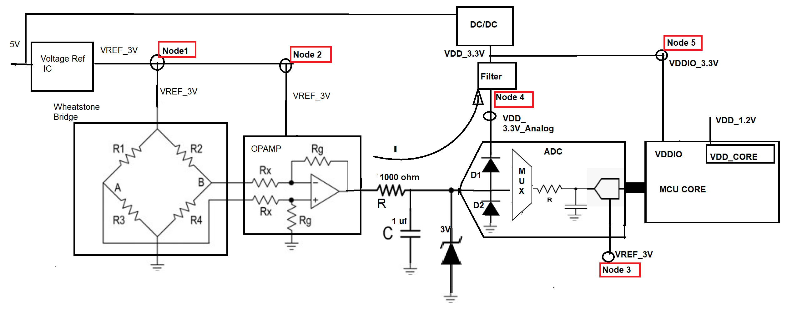
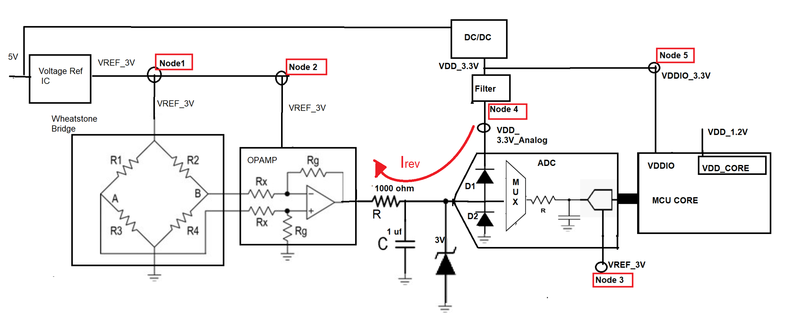
I am using  OP-AMP based sensing circuit. The OP-AMP is powered using VCC=3 V.

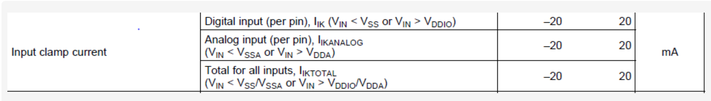
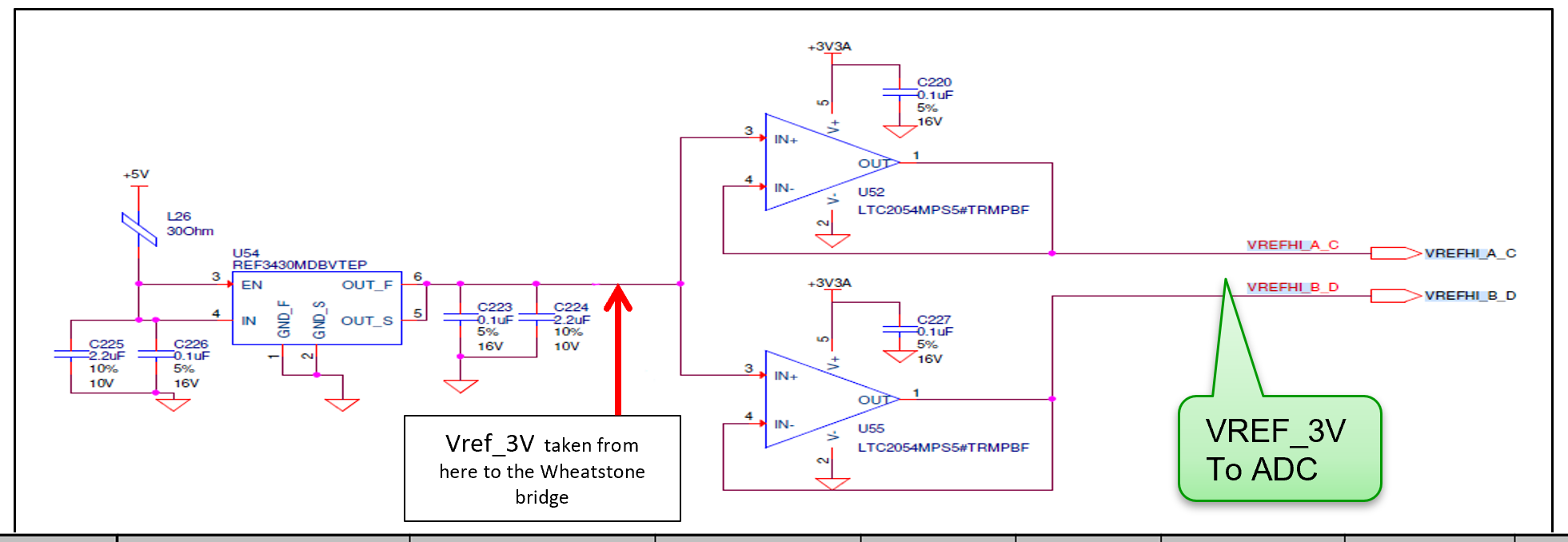
The internal ADC is used for conversion purpose which uses external reference voltage VREF_3V. 

My doubt is if the OP-AMP circuit power ups first and gives input to ADC before ADC receives the reference voltage (VREF_3V). Does it cause any damage to ADC input stage.

I am using different power supply for OP-AMP and ADC reference so it may not be synchronized. 

Reference block diagram:

Thanks,

Namita

  • Hi Namita,

    That should be fine.  The careabout should be that power 3.3V supply to the F28377 part (VDDIO and VDDA) should power up first before applying inputs to the ADC.

    Best regards,

    Joseph

  • ..

    Hi Joseph,


    To be more clear with my question I am providing following details.

    I have a RTD (R3)  based temperature sensing circuit. The Wheatstone bridge is powered using VREF_3V(Node 1) and then the output of bridge is provided to differential amplifier. The differential amplifier is powered using same VREF_3V(Node 2). The ADC is powered using VDD_3.3V (Node 4) and ADC reference using VREF_3V(Node 3).

    In order to do ratio-metric sensing I need to supply my bridge using VREF_3V , to keep the variation limited I am planning to supply the differential amplifier using VREF_3V and ADC reference also by the same supply VREF_3V.

    ADC power supply pins will get power from microcontroller power supply which is separate 3.3V DC/DC converter.

    Now my question is, Is there any need of power supply sequencing here?

    Ratio-metric is quite commonly used in many applications. If I give only the Wheatstone bridge VREF_3V and OP-AMP VDD_3.3V then the same problem can happen with OP-AMP(OPA333), As the bridge power will come before the OP-AMP power supply.

    If I use differential ADC mode of TMS320F28377D and provide the bridge output directly to ADC, then also the same issue will happen as the bridge will be powered using VREF_3V and ADC will be powered by VDD_3.3V.

    Is power supply sequencing for analog inputs absolutely necessary for TMS320F28377D for ratio-metric application?

    Is there really any danger for the multiplexer front end of the ADC ? Because power supply sequencing may add more cost and components into my design.


    Thanks,

    Namita

  • Hi Namita,

    Thank you for providing more details.  The reason why I pointed out about 3.3V supplies for the VDDA/VDDIO of F28377D being powered up first before applying inputs to the ADC channels is that the input rails for ADC belong to the 3.3V VDDA rail and having a voltage on the ADC inputs before the VDDA rail powers up would cause a current inrush to from the ADC input to the internal diode clamp when VDDA is off (0V).

    You mentioned about generation of VREF externally in your initial post.  Can you clarify that this is really going to the ADC VREFHI pins of the F28377D (node 3 in your schematics) and not the 3.3V chip supply for the F28377D (note that VREFHI pins are not the same as the VDDA terminals of the F28377D IC)?

    There is also a DCDC that supplies I presume a 3.3V level to VDD terminal of the F28377D in your schematics.  Note that VDD on the F28377D is a 1.2V rail.

    Maybe you can clarify what the VREF and VDD terminals in your schematics are.  That is where I am a bit confused.

    Best regards,

    Joseph   

  • ..

    Hi Joseph,

    I have added more detailed diagram to show all supply voltages. The additional Node 5 is the core VDD that is VDD_1.2V.


    There is anti-aliasing filter with 1 K ohm resistor R at the output of OP-AMP. So the current passing through R and D1 (When ADC is not powered) will be (3-0.2/1000=2.8 mA). 0.2 V is the forward voltage drop of diode(assumed). Is it safe now to power up the supply differently?

    The input clamp current is shown below.


    Now my question is how that Diode D1 will get forward biased if there is no voltage at its cathode.

    So I am not sure whether its zero or floating when ADC is not powered.


    Also I am using below voltage reference circuit to provide power to ADC(reference voltage) and Bridge circuit.


    The Node 1,2,3 will be provided by this reference circuit.

    So please check and suggest if this supply scheme works fine and let me know if it causes any issues.

    overall I want to know will there be any problem with this approach of proving power to different circuitry.


    Thank you,

    Namita

  • Hi Namita,

    Would you clarify what the ADC block is in your diagram?  I'm assuming that this is the representation of the ADC block of the F28377D, right?  Just wanted to make sure that it is.  If it is so, then worse case we just assume that the external DCDC is low impedance (GND) when powered off so also assuming that D1 is forward biased.  You're right, per specs, the analog input pins can sink up to 20mA so it should be ok if this is only a transient power up condition that does not last several seconds.

    On another note regarding VREF, the output of buffers U52 or U55 going to the VREFHI node 3 is fine.  What I have trouble understanding is why this same circuit is also connected to nodes 1 and 2 per your statement "The Node 1,2,3 will be provided by this reference circuit".  Maybe what you meant is that U54 is the Voltage Ref IC in your first diagram and that Node 1/2 is the one that is buffered by op amps U52/U55 which provides power to VREHI (node 3).

    Best regards,

    Joseph

  • Hi Joseph,

    Yes,  ADC block is the representation of internal ADC of the F28377D.

    On the other hand Node 1 and Node 2 are actually taken from the output of voltage reference IC U54 (The point after C224 Capacitor and before U52/U55).

    I have also indicated this point  as " Node A " after output of U54. Please refer to below diagram.

    Will there be any issues with this overall supply scheme?

    Thanks,

    Namita

  • Hi Namita,

    Thanks for the clarification.  I do not see any issues with the supply scheme.  It should work.

    Regards,

    Joseph

  • Hi Joseph,

    Thank you  for the help and support you provided.

    One more thing I would like to know about the ADC structure inside the DSP F28377D.

    So from  where we can get more details about the internal structure of the ADC inside  DSP F28377D?

    Thank you again!

    Regards,

    Namita

  • Hi Namita,

    You're welcome.  We usually do not publish the internal structures of our chips as most of these are proprietary.  The relevant parameters and topologies are typically included in the datasheets and the technical reference manuals.  If you cannot find the specific information that you are looking for in these online documents, do let me know.

    Best regards,

    Joseph

  • Hi Namita,

    Marking this thread closed for now.  If you have any further issues or queries, please post it in the forum.

    Regards,

    Joseph

  • Hi Joseph,

    Thank you so much for your continuous support.

    I have few more questions on leakage current that is flowing from ADC to OPAMP shown below as Irev.

    I am trying to get details of all possible leakage/ reverse current that will flow through R(1000 ohm) from ADC.

    Can you please provide me below details of Diode D1 reverse bias current that is Irev.

    1. Max reverse current that will flow through R(1000 ohm) from ADC
    2. Relationship between Irev and temperature like how much this reverse/linkage current gets affected by temperature.

    I assume that the possible linkage current is the reverse bias current of diode D1. But please let me know if there is any possible reverse current that may flow from ADC to OPAMP.


    Thanks,

    Namita


  • Hi Namita,

    In normal operating mode, when all the rails are powered up and input signal is being driven to the ADC input through the op-amp where ADCin < VDDA, there should not be an Irev.  The reverse actually happens where a very negligible leakage current (<<1uA across temperature) flows from the ADC input to the multiplexer.  This leakage current is insignificant to affect the conversions.

    I do however see an issue with SH (acqusition time) with the RC in front of the ADC input pin.  A 1K ohm with a 1uF shunt cap would require you to have a high SH time and would affect the ADC throughput.  You may want to move the RC in the op-amp input side instead to isolate this from the overall input impeadance as seen by the ADC.  You can refer to the example in TRM section 11.15.2 "Choosing an Acquisition Window Duration".

    Regards,

    Joseph

  • Hi Joseph,

    There is change in RC filter design the Capacitor used is 0.1 uF. And I have seen the calculations given for  the S+H time and that should be set to at least 1msec for our example.

    Regarding throughput, the analog signal is operating at very low frequency DC (0 to 5Hz) and provided to input of ADC. So we do not need high sampling rate, even 10KHz sampling frequency  is also enough.

    Do you still see an issue with the RC filter? 

    Thanks,

    Namita

  • Hi Namita,

    Reducing the cap value to 0.1uF in the RC should work for the 10kHZ sampling then.

    Regards,

    Joseph