Tool/software: Code Composer Studio
Hi,
I have to use generate PWM at different frequency depending on the value of ADC. As it is 12 bit so the max value should be 4096.
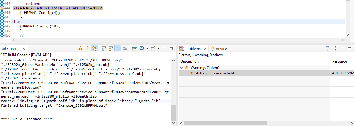
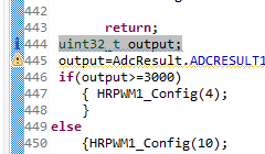
For this I have merged ADC_SoC amd HRPWM examples. And I have changed pin 4,2 to 0,1 of ADC and ePWM1 to ePWM2. I assume that ADC value is being stored in Voltage1[ConversionCount]. By providing if statement during build error is showing that this line is unreachable. It seems that it is array. How to take that variable in which ADc value is stored? I have copied ADC_SOC in HRPWM. The error line is highlighted. The error reason is given in picture
Tha main program is following
//###########################################################################
//
// FILE: Example_2802xHRPWM.c
//
// TITLE: f2802x Device HRPWM example
//
// ASSUMPTIONS:
//
//
// This program requires the f2802x header files.
//
// Monitor ePWM1 pin on an oscilloscope as described
// below.
//
// ePWM1A is on GPIO0
// ePWM1B is on GPIO1
//
//
// As supplied, this project is configured for "boot to SARAM"
// operation. The 2802x Boot Mode table is shown below.
// For information on configuring the boot mode of an eZdsp,
// please refer to the documentation included with the eZdsp,
//
// $Boot_Table
// While an emulator is connected to your device, the TRSTn pin = 1,
// which sets the device into EMU_BOOT boot mode. In this mode, the
// peripheral boot modes are as follows:
//
// Boot Mode: EMU_KEY EMU_BMODE
// (0xD00) (0xD01)
// ---------------------------------------
// Wait !=0x55AA X
// I/O 0x55AA 0x0000
// SCI 0x55AA 0x0001
// Wait 0x55AA 0x0002
// Get_Mode 0x55AA 0x0003
// SPI 0x55AA 0x0004
// I2C 0x55AA 0x0005
// OTP 0x55AA 0x0006
// Wait 0x55AA 0x0007
// Wait 0x55AA 0x0008
// SARAM 0x55AA 0x000A <-- "Boot to SARAM"
// Flash 0x55AA 0x000B
// Wait 0x55AA Other
//
// Write EMU_KEY to 0xD00 and EMU_BMODE to 0xD01 via the debugger
// according to the Boot Mode Table above. Build/Load project,
// Reset the device, and Run example
//
// $End_Boot_Table
//
// 1. PWM Freq = SYSCLK/(period=10),
// ePWM1A toggle low/high with MEP control on rising edge
// PWM Freq = SYSCLK/(period=10),
// ePWM1B toggle low/high with NO HRPWM control
//
//
//
//
/
//###########################################################################
//
// Included Files
#include "DSP28x_Project.h" // Device Headerfile and Examples Include File
#include "F2802x_Device.h" // f2802x Headerfile
#include "common/include/f2802x_examples.h" // f2802x Examples Headerfile
#include "f2802x_epwm_defines.h" // useful defines for initialization
//
// Function prototypes
//
void HRPWM1_Config(Uint16);
//%%void HRPWM2_Config(Uint16);
//%%void HRPWM3_Config(Uint16);
//%%void HRPWM4_Config(Uint16);
//ADC
__interrupt void adc_isr(void);
void Adc_Config(void);
//
// Globals
//
uint16_t LoopCount;
uint16_t ConversionCount;
uint16_t Voltage1[10];
uint16_t Voltage2[10];
//
// Globals
//
uint16_t i,j,DutyFine,n,update;
uint32_t temp;
//
// Main
//
void main(void)
{
//
// WARNING: Always ensure you call memcpy before running any functions from
// RAM InitSysCtrl includes a call to a RAM based function and without a
// call to memcpy first, the processor will go "into the weeds"
//
#ifdef _FLASH
memcpy(&RamfuncsRunStart, &RamfuncsLoadStart, (size_t)&RamfuncsLoadSize);
#endif
//
// Step 1. Initialize System Control:
// PLL, WatchDog, enable Peripheral Clocks
// This example function is found in the f2802x_SysCtrl.c file.
//
InitSysCtrl();
//
// Step 2. Initialize GPIO:
// This example function is found in the f2802x_Gpio.c file and
// illustrates how to set the GPIO to it's default state.
//
//InitGpio(); // Skipped for this example
//
// For this case, just init GPIO for EPwm1-EPwm4
//
//
// For this case just init GPIO pins for EPwm1, EPwm2, EPwm3, EPwm4
// These functions are in the f2802x_EPwm.c file
//
InitEPwm1Gpio();
//%% InitEPwm2Gpio();
//%%InitEPwm3Gpio();
//%%InitEPwm4Gpio();
//
// Step 3. Clear all interrupts and initialize PIE vector table:
// Disable CPU interrupts
//
DINT;
//
// Initialize the PIE control registers to their default state.
// The default state is all PIE interrupts disabled and flags
// are cleared.
// This function is found in the f2802x_PieCtrl.c file.
//
InitPieCtrl();
//
// Disable CPU interrupts and clear all CPU interrupt flags
//
IER = 0x0000;
IFR = 0x0000;
//
// Initialize the PIE vector table with pointers to the shell Interrupt
// Service Routines (ISR).
// This will populate the entire table, even if the interrupt
// is not used in this example. This is useful for debug purposes.
// The shell ISR routines are found in f2802x_DefaultIsr.c.
// This function is found in f2802x_PieVect.c.
//
InitPieVectTable();
//
// Step 4. Initialize all the Device Peripherals:
// Not required for this example
//
//
// For this example, only initialize the EPwm
// Step 5. User specific code, enable interrupts:
//
update =1;
DutyFine =0;
EALLOW;
SysCtrlRegs.PCLKCR0.bit.TBCLKSYNC = 0;
EDIS;
//
// WARNING: Always ensure you call memcpy before running any functions from
// RAM InitSysCtrl includes a call to a RAM based function and without a
// call to memcpy first, the processor will go "into the weeds"
//
#ifdef _FLASH
memcpy(&RamfuncsRunStart, &RamfuncsLoadStart, (size_t)&RamfuncsLoadSize);
#endif
//
// Step 1. Initialize System Control:
// PLL, WatchDog, enable Peripheral Clocks
// This example function is found in the f2802x_SysCtrl.c file.
//
InitSysCtrl();
//
// Step 2. Initialize GPIO:
// This example function is found in the f2802x_Gpio.c file and
// illustrates how to set the GPIO to it's default state.
//
//InitGpio(); // Skipped for this example
//
// Step 3. Clear all interrupts and initialize PIE vector table:
// Disable CPU interrupts
//
DINT;
//
// Initialize the PIE control registers to their default state.
// The default state is all PIE interrupts disabled and flags
// are cleared.
// This function is found in the f2802x_PieCtrl.c file.
//
InitPieCtrl();
//
// Disable CPU interrupts and clear all CPU interrupt flags
//
IER = 0x0000;
IFR = 0x0000;
//
// Initialize the PIE vector table with pointers to the shell Interrupt
// Service Routines (ISR).
// This will populate the entire table, even if the interrupt
// is not used in this example. This is useful for debug purposes.
// The shell ISR routines are found in f2802x_DefaultIsr.c.
// This function is found in f2802x_PieVect.c.
//
InitPieVectTable();
//
// Interrupts that are used in this example are re-mapped to
// ISR functions found within this file.
//
EALLOW; // This is needed to write to EALLOW protected register
PieVectTable.ADCINT1 = &adc_isr;
EDIS; // This is needed to disable write to EALLOW protected registers
//
// Step 4. Initialize all the Device Peripherals
//
InitAdc(); // For this example, init the ADC
AdcOffsetSelfCal();
//
// Step 5. User specific code, enable interrupts:
// Enable ADCINT1 in PIE
//
PieCtrlRegs.PIEIER1.bit.INTx1 = 1; // Enable INT 1.1 in the PIE
IER |= M_INT1; // Enable CPU Interrupt 1
EINT; // Enable Global interrupt INTM
ERTM; // Enable Global realtime interrupt DBGM
LoopCount = 0;
ConversionCount = 0;
//
// Configure ADC
// Note: Channel ADCINA4 will be double sampled to workaround the ADC 1st
// sample issue for rev0 silicon errata
//
EALLOW;
//
// ADCINT1 trips after AdcResults latch
//
AdcRegs.ADCCTL1.bit.INTPULSEPOS = 1;
AdcRegs.INTSEL1N2.bit.INT1E = 1; // Enabled ADCINT1
AdcRegs.INTSEL1N2.bit.INT1CONT = 0; // Disable ADCINT1 Continuous mode
//
// setup EOC2 to trigger ADCINT1 to fire
//
AdcRegs.INTSEL1N2.bit.INT1SEL = 2;
//
// set SOC0 channel select to ADCINA1
//
AdcRegs.ADCSOC0CTL.bit.CHSEL = 1;
//
// set SOC1 channel select to ADCINA1
//
AdcRegs.ADCSOC1CTL.bit.CHSEL = 1;
//
// set SOC1 channel select to ADCINA0
//
AdcRegs.ADCSOC2CTL.bit.CHSEL = 0;
//
// set SOC0 start trigger on EPWM1A, due to round-robin SOC0 converts first
// then SOC1
//
AdcRegs.ADCSOC0CTL.bit.TRIGSEL = 5;
//
// set SOC1 start trigger on EPWM1A, due to round-robin SOC0 converts first
// then SOC1
//
AdcRegs.ADCSOC1CTL.bit.TRIGSEL = 5;
//
// set SOC2 start trigger on EPWM1A, due to round-robin SOC0 converts first
// then SOC1, then SOC2
//
AdcRegs.ADCSOC2CTL.bit.TRIGSEL = 5;
//
// set SOC0 S/H Window to 7 ADC Clock Cycles, (6 ACQPS plus 1)
//
AdcRegs.ADCSOC0CTL.bit.ACQPS = 6;
//
// set SOC1 S/H Window to 7 ADC Clock Cycles, (6 ACQPS plus 1)
//
AdcRegs.ADCSOC1CTL.bit.ACQPS = 6;
//
// set SOC2 S/H Window to 7 ADC Clock Cycles, (6 ACQPS plus 1)
//
AdcRegs.ADCSOC2CTL.bit.ACQPS = 6;
EDIS;
//
// Assumes ePWM1 clock is already enabled in InitSysCtrl();
//
EPwm2Regs.ETSEL.bit.SOCAEN = 1; // Enable SOC on A group
//
// Select SOC from from CPMA on upcount
//
EPwm2Regs.ETSEL.bit.SOCASEL = 4;
EPwm2Regs.ETPS.bit.SOCAPRD = 1; // Generate pulse on 1st event
EPwm2Regs.CMPA.half.CMPA = 0x0080; // Set compare A value
EPwm2Regs.TBPRD = 0xFFFF; // Set period for ePWM1
EPwm2Regs.TBCTL.bit.CTRMODE = 0; // count up and start
//
// Wait for ADC interrupt
//
for(;;)
{
LoopCount++;
}
}
//
// adc_isr -
//
__interrupt void
adc_isr(void)
{
//
// discard ADCRESULT0 as part of the workaround to the 1st sample errata
// for rev0
//
Voltage1[ConversionCount] = AdcResult.ADCRESULT1;
Voltage2[ConversionCount] = AdcResult.ADCRESULT2;
//
// If 20 conversions have been logged, start over
//
if(ConversionCount == 9)
{
ConversionCount = 0;
}
else
{
ConversionCount++;
}
//
// Clear ADCINT1 flag reinitialize for next SOC
//
AdcRegs.ADCINTFLGCLR.bit.ADCINT1 = 1;
//
// Acknowledge interrupt to PIE
//
PieCtrlRegs.PIEACK.all = PIEACK_GROUP1;
return;
if(Voltage1[Conversioncount]>3000)
{ HRPWM1_Config(4);
}
else
{HRPWM1_Config(10);
}
//
// Some useful Period vs Frequency values
// SYSCLKOUT = 60 MHz
//
// Period Frequency
// 1000 60 kHz
// 800 75 kHz
// 600 100 kHz
// 500 120 kHz
// 250 240 kHz
// 200 300 kHz
// 100 600 kHz
// 50 1.2 Mhz
// 25 2.4 Mhz
// 20 3.0 Mhz
// 12 5.0 MHz
// 10 6.0 MHz
// 9 6.7 MHz
// 8 7.5 MHz
// 7 8.6 MHz
// 6 10.0 MHz
// 5 12.0 MHz
//
// ePWM and HRPWM register initialization
//
// ePWM1 target, Period = 4
EALLOW;
SysCtrlRegs.PCLKCR0.bit.TBCLKSYNC = 1;
EDIS;
while (update ==1)
{
for(DutyFine =1; DutyFine <256 ;DutyFine ++)
{
//
// Example, write to the HRPWM extension of CMPA
//
//
// Left shift by 8 to write into MSB bits
//
EPwm1Regs.CMPA.half.CMPAHR = DutyFine << 8;
//
// Left shift by 8 to write into MSB bits
for (i=0;i<10000;i++)
{
//
// Dummy delay between MEP changes
//
}
}
}
}
//
// HRPWM1_Config -
//
void
HRPWM1_Config(Uint16 period)
{
//
// ePWM1 register configuration with HRPWM
// ePWM1A toggle low/high with MEP control on Rising edge
//
EPwm1Regs.TBCTL.bit.PRDLD = TB_IMMEDIATE; // set Immediate load
EPwm1Regs.TBPRD = period-1; // PWM frequency = 1 / period
EPwm1Regs.CMPA.half.CMPA = period / 2; // set duty 50% initially
EPwm1Regs.CMPA.half.CMPAHR = (1 << 8); // initialize HRPWM extension
EPwm1Regs.CMPB = period / 2; // set duty 50% initially
EPwm1Regs.TBPHS.all = 0;
EPwm1Regs.TBCTR = 0;
EPwm1Regs.TBCTL.bit.CTRMODE = TB_COUNT_UP;
EPwm1Regs.TBCTL.bit.PHSEN = TB_DISABLE; // EPwm1 is the Master
EPwm1Regs.TBCTL.bit.SYNCOSEL = TB_SYNC_DISABLE;
EPwm1Regs.TBCTL.bit.HSPCLKDIV = TB_DIV1;
EPwm1Regs.TBCTL.bit.CLKDIV = TB_DIV1;
EPwm1Regs.CMPCTL.bit.LOADAMODE = CC_CTR_ZERO;
EPwm1Regs.CMPCTL.bit.LOADBMODE = CC_CTR_ZERO;
EPwm1Regs.CMPCTL.bit.SHDWAMODE = CC_SHADOW;
EPwm1Regs.CMPCTL.bit.SHDWBMODE = CC_SHADOW;
EPwm1Regs.AQCTLA.bit.ZRO = AQ_CLEAR; // PWM toggle low/high
EPwm1Regs.AQCTLA.bit.CAU = AQ_SET;
EPwm1Regs.AQCTLB.bit.ZRO = AQ_CLEAR;
EPwm1Regs.AQCTLB.bit.CBU = AQ_SET;
EALLOW;
EPwm1Regs.HRCNFG.all = 0x0;
EPwm1Regs.HRCNFG.bit.EDGMODE = HR_REP; // MEP control on Rising edge
EPwm1Regs.HRCNFG.bit.CTLMODE = HR_CMP;
EPwm1Regs.HRCNFG.bit.HRLOAD = HR_CTR_ZERO;
EDIS;
}
//
// End of File
//