


Hi
This is a two-level structure of the 2KW DC project: pre-Boost + post-PSFB. Separately debug single-stage load to the full power of 2KW work, all normal. During joint debugging, when the output is brought to 14V / 100A, the front-stage boost driver is turned off.
Experiment 1:
PWM interrupt 100k pin flip signal CH3 does not flip (set the input interrupt high, and the output interrupt low), the experimental waveforms are shown in the attachment (wf_353, wf_352).
wf_353:
wf_352:

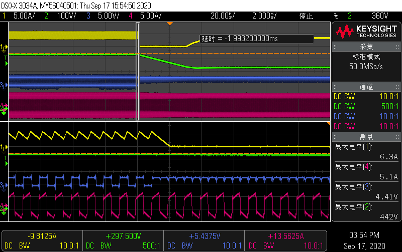
1.1) Test conditions: Vin=330VDC, Vo=13.9V, CC=30A, cut load to CC=100A;
1.2) Oscilloscope channel description:
CH1: Boost inductor current;
CH2: Bulk voltage (Boost output voltage);
CH3: Bulk_POK (100kHz flip signal, used to determine whether the DSP is down);
CH4: Resonant inductor L6 current waveform;
Supplement: After the Bulk_POK pin is toggled in the main program, when the DSP is turned off, the signal still does not flip.
Experiment 2:
After the PWM is turned off abnormally, test VDD=1.8V, VDDIO=3.3V, and XRS (PIN3) high level. --normal.

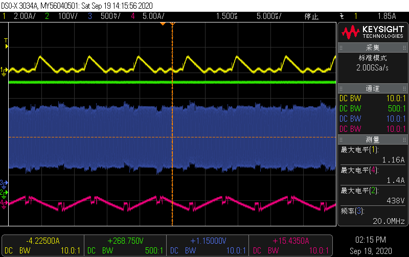
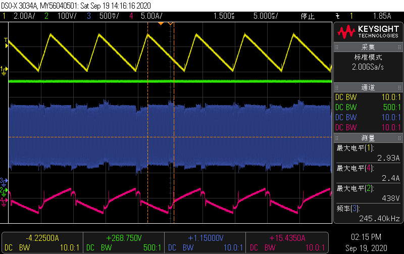
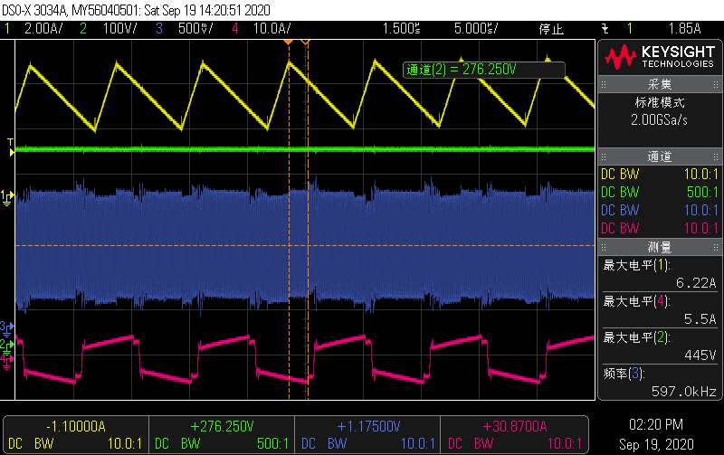
Experiment 3:
After abnormally turning off the PWM, measure the crystal oscillator.
CH1: Boost inductor current; CH2: Bulk voltage; CH3: C817 (20MHz crystal oscillator); CH4: Resonant inductor L6 current waveform;
Vin=330VDC, Vo=13.9V, CC=30A cut load to CC=100A;
No load wf_380
CC=30A wf_381
CC=100A wf_382
Thank you!

