This thread has been locked.

If you have a related question, please click the "Ask a related question" button in the top right corner. The newly created question will be automatically linked to this question.

TMS320F28335: AD problem of TMS320F28335

Part Number: TMS320F28335

Dear Expert,

Pls help check my falure case, Thank you.

AD problem of DSP

TMS320F28335PGFA

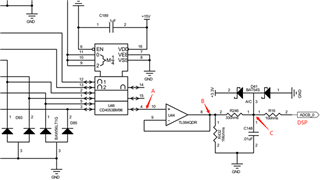
Fault phenomenon: running for a period of time, the signal appears abnormal: The basic circuit is as follows:

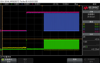
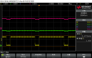
Under normal circumstances, the waveforms of A, B and C are the same, as below:

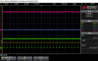
Yellow and Green are the waveforms for point A and C, Blue is the gating control signal from Analog switch CD4053, and Red is the +15V power supply. The expansion diagram as below:


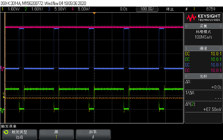
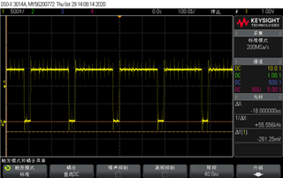
Waveform when failure: Yellow is point A, Red is point B, Green is point C, Blue is analog switch CD4053 gate control:


It seems that the output of the op-amp is pulled up from +1.5V to 1.7V and 0V to 1.5V. After R246, point C is pulled up to the voltage between 2.5V and 2.6V, as below:


When failure, disconnected signals of R16, then signals of Point A, B and C were all restored to normal status, and the ADCB_0 signal sent to DSP was changed to +3.3V.


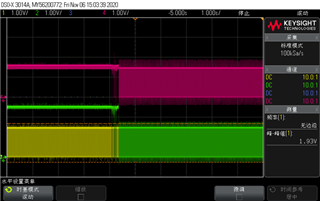
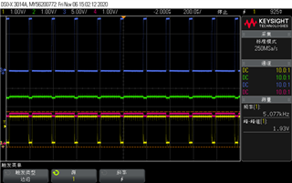
Failure startup waveform: Yellow is point A, Green is point C, Blue is analog switch selection signal, Red is point B.

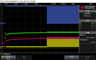
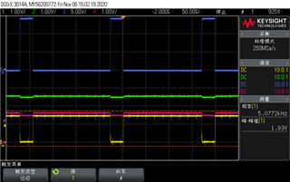
Normal startup waveform: Yellow is point A, Green is point C, Blue is analog switch selection signal, Red is point B. Red is +15V power supply.

  • Derek,

    Thanks for reaching out to the E2E.

    From your description of what occurs on the ADC input channel during the failure(always converting 4096) as well as removing the resistor R16 I think the ADC pin of the F28335 may be under the influence of another channel.

    Can you look at the other ADC inputs(esp if they are on the B, but even the A) and see if any of those pins is 0.7V > VDDA/3.3V?  The mux selection switch inside this device is a simple Pchannel and Nchannel in parallel, but if there is too large a voltage it will reverse bias the mux and feed back the other ADC channels.

    My other thought is that the built in ESD structure is clamped on ADCINB0, but I don't see an overvoltage on this pin from your scope plots.

    Best,

    Matthew

  • Dear  Matthew,

    What's the meaning of 0.7V > VDDA/3.3V and we have a clamp protection diode on each AD sampling channel, Thank you.

    This is my key customer, could you mail to me(derek.zhong@arrow.com)? I will loop customer in mail, Thank you.


  • Derek,

    I'll loop you in offline as requested; and we can post back here once we understand root cause.

    Best,

    Matthew