This thread has been locked.

If you have a related question, please click the "Ask a related question" button in the top right corner. The newly created question will be automatically linked to this question.

F28M35H52C: F28M35x First Power-On - Unexpected Pulses on XRS/ARS Pins

Part Number: F28M35H52C

Hi,

I'm working with F28M35H52C Concerto device installed on our custom-designed application hardware. This is a new design and we performed the first power-up test with no any code loaded to the device so the Concerto device is in its initial off-the-shelf condition. With all the power voltages applied and no signs of overload I started checking the reset signals on the XRS/ARS reset pins. These pins are connected together as recommended by the device documentation. I've found the unexpected pulses on these pins that are only present if device attempts to boot into flash memory. If boot mode is changed to serial interface, these pulses disappear and nXRS = 1 as expected.


My thought is that these reset pulses are triggered by one of the watchdog timers. Upon checking the TRM I've found that WDT1 and WDT0 timers are disabled by default and therefore it's my take that resets are triggered by NMI WDT. But here is where my confusion comes.

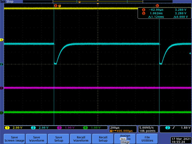
The X1 clock in our application is 20 MHz so the clock period is 50 ns. Based on the nXRS waveform provided above, the reset pulse period is 1.124 ms. But, given that NMI WDT is 16-bit counter, I would anticipate that period to be 50ns * 2^16 = 3.2768 ms, which is about 3X the observed period. I'm not sure if it takes 1 or 2 NMI WDT cycles to trigger system reset but the observed period is just the fraction of even a single cycle.

So my questions are as follows below.

Q1: Is it correct that the observed nXRS pulses are caused by the NMI WDT timer? If not, what's the possible source?

Q2: If these pulses are indeed caused by the NMI watchdog, then why is there a discrepancy between the anticipated and observed period values?

Thank you,
Michael

  • Michael,

    I agree that this seems to be the NMI WD timer, but as you mention based on a 20MHz clock on X1 the time between low pulses is too short. 

    However, the active low time on XRSn for the NMI WD is 512 osc clocks ~ 26us which does seem to agree with the scope plot.

    I need to reach out to some colleagues to understand why we are 3X the rate and give you a solid answer, even though we are both fairly certain this is the WD mechanism.

    Best,

    Matthew

  • Thank you, Matthew.

    Please let me know once you have more information.

    Regards, Michael

  • Hi Matthew,

    Have you had a chance to check with your colleagues regarding the timing discrepancy above? Please let me know the findings. We still don't have any definitive answer and that starts affecting our project flow. Your attention to this matter is highly appreciated.

    Regards, Michael

  • Michael,

    My current thought is that the erased flash, when executed as part of a boot to flash, will cause a bus fault exception since this would be an invalid instruction, as well as the ECC not being programmed.

    Would it be possible to place some small code, even like one of the examples from our support package to see if this goes away?  Even code that purposefully doesn't disable the main WDs(all of our examples would disable/service the WD) so that we could see that come out at the expected frequency.

    Just some clarification on an original statement, the main WDs are disabled for the peripheral booting modes, since there is going to be some different delays depending on the implementation.  However, these are enabled for flash boot mode, since code execution should be known.

    Best,

    Matthew

  • Matthew,

    Thank you for your response. No, for several reasons it won't be possible to load any code into the board at the moment. Your idea about watchdog being enabled for boot-to-flash is probably confirmed indirectly since problem disappears if boot-to-serial interface is configured. However, I couldn't find confirmation of that behavior in the TRM. Could you please point me to the relevant explanation in that document?

    What is confusing is that WDT0 and WDT1 are 32-bit timers and out of reset they're configured to run the full length cycle if enabled, which is much longer than 1.124 ms we observe on the waveform above. So, to get 1.124 ms period, any WDT must be reconfigured appropriately. That would require setting appropriate WDTLOAD value for WDT0 or WDT1 or MNMIWDPRD value for NMI WDT. And the question now is if such a reconfiguration really occurs as a part of boot-to-flash process. Is that what is really happening? That would also answer my original Q2 question.

    Please advise.

    Regards,
    Michael

  • Michael,

    I believe I found the reason here.  From the F28M35 TRM:

    So when we jump to erased flash, we trigger a bus fault exception and per above in the BROM this will in turn trigger a Hard Fault Exception.

    I looked at this ISR, and it is set to trigger a WD Reset after a very short delay of 256 cycles once it is called.  This would explain the non typical time duration between reset pulses you are seeing when booting to erased flash, since it is not based on a 32-bit timeout.

    Based on the code snippet, my statement on WD being enabled was incorrect.  I don't believe that the WD is enabled by the Boot ROM for any bootmode including the flash.

    void mbrom_hard_fault_isr_handler()
    {
    	mbrom_boot_status_to_app |= M_BOOTROM_STATUS_TO_APP_HARD_FAULT_EXCEPTION;
    
    	/*in certain cases RAM might not be accessible, so don't use function calls
    	 * instead write to peripheral directly
    	 */
    	EALLOW;
    	HWREG(SYSCTL_RCGC0) |= SYSCTL_RCGC0_WDT0;	//enable clock to WatchDOG
    	//enable watchdog
    	HWREG(WATCHDOG0_BASE + WDT_O_CTL) |= WDT_CTL_INTEN;
    	//load watchdog with a small value for immediate reset
    	HWREG(WATCHDOG0_BASE + WDT_O_LOAD) = 0x100;
    	// Enable the watchdog reset.
    	HWREG(WATCHDOG0_BASE + WDT_O_CTL) |= WDT_CTL_RESEN;
    	EDIS;
    	while(1);
    }

    Best,
    Matthew

  • Hi Matthew,

    Thank you for your response. So based on the fact that WDT0 generates reset on the second time-out and given the 512 clock cycles for the pulse width itself, we now have the time interval of 1024 = (2x256 + 512) clock cycles or, for 20 MHz X1 clock, 51.2us time. Since the reset pulse period is about 1.124 ms, it leaves us with 1.0728ms time interval still unaccounted for.

    Q3: Is it safe to assume that the remaining 1.0728ms time interval represents the M-Boot execution time starting from the reset pulse and up to the moment the Hard Fault ISR handler is started?

    Regards,
    Michael

  • Michael,

    Yes that was my conclusion as well.  Keep in mind that since the PLL is not yet enabled we'll be executing at 20MHz clock, which explains the longer duration of time here.

    I'll bring up an earlier comment I made, the hold low time of the XRSn pulse also corresponds to the DS of 512 OSC Clock cycles.  So this is definitely the WD asserting a reset.

    Best,

    Matthew

  • Thank you, Matthew.
    Let's take it as a final answer for now.