This thread has been locked.

If you have a related question, please click the "Ask a related question" button in the top right corner. The newly created question will be automatically linked to this question.

BOOSTXL-BUCKCONV: Compensation for closed loop PCMC and VMC (default location of poles and zeros)

Part Number: BOOSTXL-BUCKCONV
Other Parts Discussed in Thread: SFRA

Hi, 

The default compensation for closed loop PCMC is Z0 = 0.0001kHz, Z1 = 25kHz and P1 = 3kHz. I believe the current mode requires only 1 pole and 1 zero for compensation. while the DCL22 means two pole and two zeros. Could you please explain the values of zero and pole used by default. what does Z0 value mean here? It is too low. And Z1 and P1 values also seem to be odd having zero after the pole.

Also in VMC, I can only see two zero and one pole in the code. where is the second pole placed?

Thanks,

Ajit

  • Ajit,

    The first pole of DF22 is fixed to 0Hz by design. You can see this inference in the Compensation Designer GUI, where fp0 shows as 0 and cannot be modified. The DCL User's Guide also shows the underlying behavioral equation if you prefer to think in those terms.

    PID is the highlighted compensation load model for PCMC. An acceptable set of default ZPK load values was found through empirical iteration with Compensation Designer for the sake of having a safe operating point, rather than through mathematical derivation for optimal placement.

    In practice, I would consider Z1=25kHz to have minimal influence as it is placed beyond the bandwidth of the system. Z0=0.1Hz is effectively zero and helps to cancel P0 at 0Hz. So this leaves P1=3kHz as the primary tuning vehicle.

    -Tommy

  • Hi Tommy,

    Thanks for the clarification. Could you please help me with below doubts I have. 

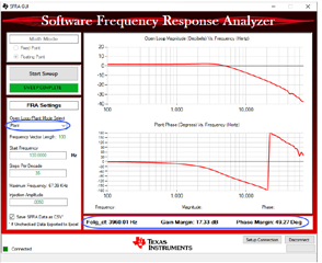
    1. In the Plant Bode plot, why is the Plant Bode plot has 0dB DC Gain. It should be actually VIN (9V) in magnitude which means around 19 dB.

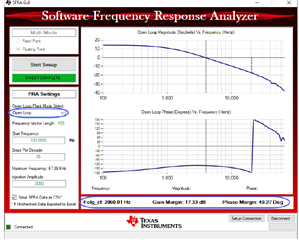
    2. In the open loop VMC case, the plant and open loop should actually mean the same thing? Why are the Bode plots different here ( see below)

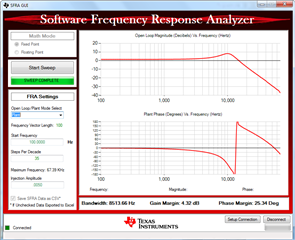
    3. Also, the plant should have double pole due to LC which clearly does not look like here. If ESR zero is close the pole then the phase lag should be not 180 degree which is also not the case here. Please explain this too


  • Thanks for the clarification. Could you please help me with below doubts I have. 

    I would recommend also reviewing the SFRA documentation for details of how it is implemented.

    In the Plant Bode plot, why is the Plant Bode plot has 0dB DC Gain. It should be actually VIN (9V) in magnitude which means around 19 dB.

    The SFRA inputs and graph are abstracted into per-unit values. The absolute magnitudes of the control and Vout levels would need to be calculated based on the control and feedback gains.

    2. In the open loop VMC case, the plant and open loop should actually mean the same thing? Why are the Bode plots different here ( see below)

    3. Also, the plant should have double pole due to LC which clearly does not look like here. If ESR zero is close the pole then the phase lag should be not 180 degree which is also not the case here. Please explain this too

    I'll ask some colleagues to provide input.

  • Ajit,

    Regarding the double-pole, I was informed that the electrolytic capacitor on Vout is interfering with the characteristic plant behavior.  The plot has a more traditional appearance when the cap is removed:

    -Tommy

  • Ajit,

    With respect to SFRA Open-Loop vs Plant, I was informed that the SFRA calculations make assumptions that are only applicable to systems that are running in Closed-Loop operation.  When running the system in Open-Loop operation, the assumptions produce artifacts.

    -Tommy