This thread has been locked.

If you have a related question, please click the "Ask a related question" button in the top right corner. The newly created question will be automatically linked to this question.

TMS320F280049: Analog input current draw and behavior

Part Number: TMS320F280049
Other Parts Discussed in Thread: LAUNCHXL-F280049C, DRV8320

My question is similar to the one in this post: "TMS320F280049: Electrical characteristics difference on F280049’s analog pins"

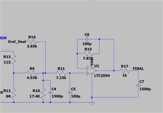
My hardware has identical analog inputs, but for some reason, one of them is behaving differently than the others. There are inputs measuring 3 motor phase currents. The circuit is represented here as shown below where R12 represents the burden resistor of the hall effect sensor, Vref_final = 3.3V, Vdd = 3.3V and the voltage across C7 goes into the A2D input on the processor. When no current is flowing the voltage across C7 = 1.65V ideally. 

So here is the issue. I have 3 channels setup with this same circuit. Those channels are connected from my hardware to the LAUNCHXL-F280049C header pins (27, 28, 29) which map as follows to the processor inputs.

Header pin 27 = Processor pin 38 (A9) and pin 16 (PGA5_IN)

Header pin 28 = Processor pin 19 (C0) and pin 20 (PGA3_IN)

Header pin 29 = Processor pin 7 (B2/C6/PGA3_OF) and pin 18 (PGA1_IN)

When the launchpad is connected, the voltage at header pin 27 is about 40mV lower than the other two pins. As best I can tell the channels are setup the same way in firmware. So for example, here is what I measured when there is zero motor phase current and the launchpad is connected.

Header pin 27 = 1.612V

Header pin 28 = 1.647V

Header pin 29 = 1.645V

And when the launchpad is disconnected from the headers, here is what I measure at the same header locations.

Header pin 27 = 1.648V

Header pin 28 = 1.647V

Header pin 29 = 1.645V

What is different about this analog input relative to the other two? What should I look at in the firmware that might affect how this channel behaves relative to the other channels. I simulated the ADC input to ensure that during sampling I get good settling with the assumptions about the sampling circuit in the datasheet, but if there is something else drawing current on these lines (such as something related to the PGAs) then I need to be able to account for that (or disable it) when selecting and RC value for these inputs. And an even more general question, what is the maximum recommended source resistance on the ADC channels? I assumed input impedance could be a few kOhm because of the relatively high source impedances used for the analog voltage feedback inputs on your DRV8320 and 3PHGAN eval kits.

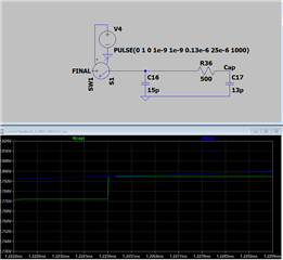
Here are the simulation results I referred to above. The voltage at node "FINAL"  is connected to the output of the opamp circuit above. The image quality become poor when I imported it, but you can generally see the behavior. The plot is zoomed in on a single sample of a sine wave (blue). The waveform (green) settles in within a reasonable about the time and within the sampling interval we have for the ADC. 

Blue Waveform = Sine Wave measured at "FINAL" node.

Green Waveform = ADC sampled waveform measured across C17 ("Cap" node).

Thanks.

  • Hi Gabe,

    I think issue is on the impedance seen by the ADC at the 'FINAL' node.  Just doing some calculations here based on the values from your schematic diagram using the example in the section "Choosing an Acquisition Window Duration" and the parasitics, mux resistance and sampling capacitor values from the datasheet available  on the "ADC Input Model" section:

    Time constant (tc):

         tc = (1000 + 500)*12.6pF + 1000*(1500pF + 8.1pF) = 1.53uS

    Number of time constants required assuming ¼ LSB settling (k):

         k = ln(4096/0.25) – ln ((1500pf + 8.1pF)/12.6pF) = 9.704 – 4.785 = 4.919

    Sample and hold time (SH):

         SH = k.tc = 1.53uS*4.919 = 7.5uS

     Typical SYSCLK for F280049 running at specification:

         period = 1/SYSCLK = 1/100MHz = 10nS

    Register setting for SH (ACQPS):

         ACQPS = SH/period – 1 = 7.5uS/10nS = 749

    This is where the problem lies.  The ACQPS register is 9 bits wide, which allows for a maximum of 511 SYSCLK cycles.  The effect of having high values of source impedance (in your case R17 and C7) is higher sample and hold times.  Based on R17/C7 values, signals need to settle at 7.5uS to allow the SAR sampling capacitor to settle to within ¼ of an LSB, and even if you max out ACQPS to 511 which is 5.12uS, that is not allowing enough time for the sample and hold capacitor to fully charge.

     Couple of options to try:

         - Reduce the values of R17/C7 and rerun the calculations to ensure SH is sufficient so that ACQPS will be able to accommodate the new SH value

         - If R17/C7 are needed (probably for low pass filtering), move that filtering before the input of the op amp.  This might require you to recalculate the other R’s and C’s around the opamp and still maintain the gain and BW that your circuit requires.

    Regards,

    Joseph

  • I did the same calculations already but abandoned them in favor of a simulation because they do not account for the contribution of the 1500pF cap as it acts like a source over short sampling windows. A simulation is recommended by the same page of the app note, SPRUI33D p.1470, that has these calculations and is as follows "While this gives a rough estimate of the required acquisition window, a better method would be to setup a circuit with the ADC input model, a model of the source impedance/capacitance, and any board parasitics in SPICE (or similar software) and simulate to verify that the sampling capacitor settles to the desired accuracy."

    I plan to reduce the RC as you suggested but it still dost explain why only 1 of the 3 channels has the issue when all 3 are the same values of RC. There must be something else going on creating this voltage drop. Can you check with your colleagues on this? Do the ADC channels route anywhere else inside the part that could be drawing current on the order of 40uA? Thanks.

  • Hi Gabe,

    Sorry, I just realized that you were using the ADC channels that were connected to the PGA_INx through 0ohm resistors  R20, R17 and R14. In this case, the signal goes to the ADC channel as well as PGA_INx.  I assume you are not configuring the PGAs in your code and just doing the signal conversion on ADC channels A0, C0, and B2.  Analog pin internal connections are all documented and tabulated in Table 7-11 and shows connections to the AD input mux, PGAx , comparators and DACs.

    Can you try connecting the FINAL taps into ADC channels that are not connected to PGA to see if issue will persist, or depopulate R20, R17 and R14 in the launchpad to isolate it from the PGA inputs?

    Regards,

    Joseph

  • Hi Gabe,

    Also to add PGA inputs do not work as unity gain amplifiers (buffer) for external current monitors output centers via 1.65v reference. You have to use PAG_OF inputs and change the analog MUX as Joseph mentions to use CCMPx for EPWM trip zone events. I wasted day trying to get similar input buffer (PGA) to work and TI Kevin hinted the PGA output would not center 1.65v via non-inverting PGA_+IN.