


I am having difficulty understanding how I should extrapolate from the examples and literature which fall short of describing a solution to the problem in the subject - these descriptions instead involve RUNNING from FLASH everything except the InitFlash routine which is used to establish FLASH execution paramters, of necessity before execution of the rest of the entirety of the program from FLASH.
Should a seprate Code Section be created for each function in the program (each function is to run from RAM) ?
Using the JTAG and the debugger to progam FLASH and then Run is the same as cycling power with BOOT pins (GPIO 84, 85, 86, 87- Control Card Rev 1.1 TMDSCNCD28335PGF ) set high ? Or will booting from FLASH after a power cycle behave differently from the use of the emulator/debugger to load and run where booting from FLASH will actually load the entire program to RAM ?
Are jumpers actually required on GPIOs 84, 85, 86, 87 to set the GPIO inputs to HIGH for booting ? Whereis teh description of which if the 3 pins for each GPIO to use to pull high vs which to pull low ?
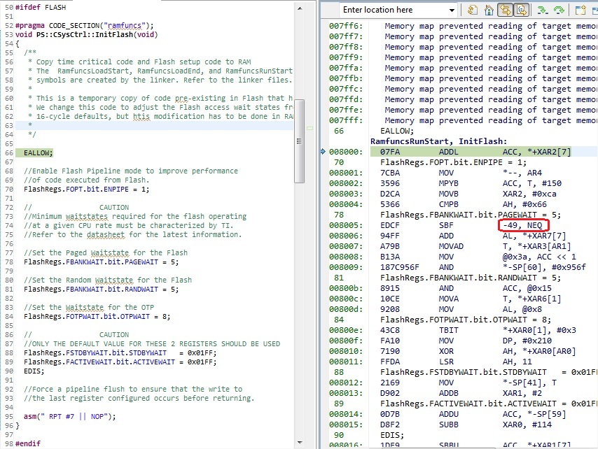
And finally I can not get InitFlash to execute correctly - loads to RAM but upon reaching statement to set first Wait State the instruction appears to want to take execution backwards 49 memory locations to make the wait state value assignment - only problem is that since we are now in RAM rather then FLAS where the InitFlash routine was program/loaded there is no statement there in RAM while there might have been such a statement in FLASH.


