Other Parts Discussed in Thread: TMS320F28335
Hi,
I am running into some problems with transmission when running the TMS320F28335
as an SPI slave.
I am using the SPIA port as slave, 8 bit word. LSPCLK = 75MHz. I am running the master SPICLK at
500 kHz to make sure that I am not encountering a timing issue.
1.- Reads from RXBUF are right aligned, writes to TXBUF are left aligned.
2.- RX and TX Buffers are enabled. RX FIFO level is 1, TX FIFO level is 0.
3.- When the system starts RXFFIENA is enabled, TXFFIENA is disabled
The DSP is emulating an EEPROM; When I do a read sequence I get the following
sequence of events.
<-- Master lowers #SPISTEA
<-- Master sends command byte ( SPICKL cycles 1..8 );
--> RXINT triggers in the DSP, the command is read from RXBUF and processed.
<-- Master sends address byte ( SPICKL cycles 9..16 );
--> RXINT triggers in the DSP, the adress is read from RXBUF and processed.
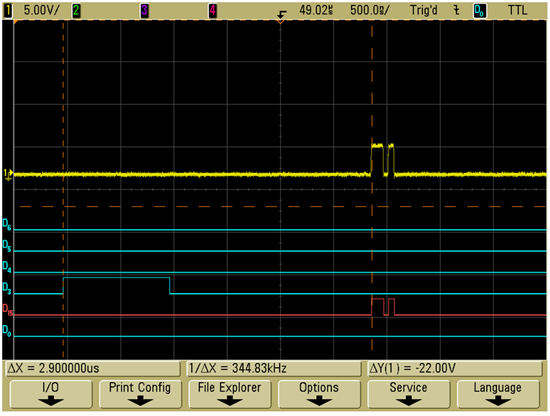
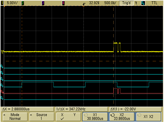
DSP writes 2 bytes into TXBUF and then enables the TXFFIENA
<-- Master drives SPICLK and keeps SPISTEA low ( SPICKL cycles 17..24 )
I would expect the first byte that I wrote into TXBUF to appear in the SOMI line
during SPICKL edges 17..24, but I get garbage instead (it is always the same
word)
<-- Master drives SPICLK and keeps SPISTEA low ( SPICKL cycles 25..32 )
I get the second byte that I wrote into TXBUF in the SOMI line
--> When TX int triggers I copy two new bytes to the TXBUF
(in fact my application is a read sequence of 20 bytes - master will keep the
SPICLK running - but I get 19 out, as I miss the 1st one, but it also seems that
the last byte remains in the queue, because I get it at the beginning of the
next read sequence).
---
Any idea what can be causing that the first byte is not getting transmitted?
Not enough time between the RXINT and the writing of the first byte in TXBUF?
---
Below is my configuration of the SPI
SpiaRegs.SPICCR.bit.SPISWRESET = 0;
// set SPI Configuration Control Register
SPICCR_REG shadowSPICCR;
shadowSPICCR.all = 0;
shadowSPICCR.bit.SPISWRESET = 0; // Initializes the SPI operating flags to the reset condition
shadowSPICCR.bit.CLKPOLARITY = 0; // shift clock polarity (mode 00)
shadowSPICCR.bit.SPICHAR = 0x7; // character length control bits
SpiaRegs.SPICCR.all = shadowSPICCR.all;
// set SPI Operation Control Register
SPICTL_REG shadowSPICTL;
shadowSPICTL.all = 0;
shadowSPICTL.bit.OVERRUNINTENA = 0; // enable receiver overrun interrupts
shadowSPICTL.bit.CLK_PHASE = 0; // normal SPI clocking scheme (mode polarity 0 - phase 0)
shadowSPICTL.bit.MASTER_SLAVE = 0; // SPI configured as slave
shadowSPICTL.bit.TALK = 1; // enable data transmission
shadowSPICTL.bit.SPIINTENA = 1; // enable SPI interrupts
SpiaRegs.SPICTL.all = shadowSPICTL.all;
// set SPI TX FIFO register
// Reset the Tx Fifo
SPIFFTX_REG shadowSPIFFTX;
shadowSPIFFTX.all = 0;
shadowSPIFFTX.bit.SPIRST = 1; // SPI FIFO can resume TX and RX
shadowSPIFFTX.bit.SPIFFENA = 1; // enable SPI FIFO
shadowSPIFFTX.bit.TXFIFO = 0; // enable TX FIFO
shadowSPIFFTX.bit.TXFFINTCLR = 1; // clear TX FIFO interrupt flag
shadowSPIFFTX.bit.TXFFIENA = 0; // do not enable TX FIFO interrupt, until there is something to send
shadowSPIFFTX.bit.TXFFIL = 0; // TX FIFO level
SpiaRegs.SPIFFTX.all = shadowSPIFFTX.all;
// set SPI RX FIFO register
SPIFFRX_REG shadowSPIFFRX;
shadowSPIFFRX.all = 0;
shadowSPIFFRX.bit.RXFFOVFCLR = 1; // clear RX FIFO overflow flag
shadowSPIFFRX.bit.RXFIFORESET = 1; // enable RX FIFO
shadowSPIFFRX.bit.RXFFINTCLR = 1; // clear RX FIFO interrupt flag
shadowSPIFFRX.bit.RXFFIENA = 1; // enable RX FIFO interrupt generation based on level
shadowSPIFFRX.bit.RXFFIL = 1; // RX FIFO level
SpiaRegs.SPIFFRX.all = shadowSPIFFRX.all;
// set SPI FIFO Control register
SpiaRegs.SPIFFCT.all = 0;
// set SPI Priority Control Register
SPIPRI_REG shadowSPIPRI;
shadowSPIPRI.all = 0;
shadowSPIPRI.bit.FREE = 1; // 11 mode -
shadowSPIPRI.bit.SOFT = 1; //
SpiaRegs.SPIPRI.all = shadowSPIPRI.all;
// Relinquish SPI from Reset
SpiaRegs.SPICCR.bit.SPISWRESET = 1;
SpiaRegs.SPIFFTX.bit.SPIRST = 0; // Reset the TX & RX Buffers
SpiaRegs.SPIFFTX.bit.SPIRST = 1;
SpiaRegs.SPIFFTX.bit.TXFIFO = 1; // Enable the FIFO


