This thread has been locked.

If you have a related question, please click the "Ask a related question" button in the top right corner. The newly created question will be automatically linked to this question.

NEW Delfino F2837xD Series: Up to 800 MIPS and 16-bit ADC

Other Parts Discussed in Thread: TMDSADAP180TO100, CONTROLSUITE, TMS320F28377D, OMAPL138

Key Features

  • Dual-core C28x at 200 MHz each
  • Floating Point Unit
  • NEW Trigonometric math unit (TMU)
  • ENHANCED Viterbi Complex Unit (VCU)
  • Two programmable 32-bit floating-point real-time accelerators (CLAs) on chip
  • Up to 1 MB of Flash
  • Dual DMA controllers
  • Dual EMIFs and uPP Interface
  • High Resolution PWMs (down to 55ps)
  • NEW 4x 16 bit ADCs, 1 MSPS
  • NEW Windowed Comparators
  • 32-bit QEP and Capture modules
  • Programmable PWM Trip

Order controlCARDs and Experimenter's Kits, shipments within 2 weeks!

Check out the Delfino Site or the F2837xD Product Folder for more information.


  • Great news... Looking forward to work with one! 

  • Interesting!

    When will be available at distributors?

    And schematics of controlCard and TMDSADAP180TO100?

    ^_^

  • TC,

    www.ti.com/tool/controlsuite

    latest update has

    C:\ti\controlSUITE\development_kits\~controlCARDs\TMDSADAP180TO100_v1_0\R1_1

    C:\ti\controlSUITE\development_kits\~controlCARDs\TMDSCNCD28377D_v1_0\R1_1

    controlCARDs and adapters are stocking up in our distribution center, so distis can place orders now, or purchase through eStore.


  • Chris,

       I especially liked of the flash with only 20 ns access time (100MHZ with only one wait state)

       High-Resolution on Both A and B Outputs.

       Can we expect these innovations to the next Piccolo in 2014?


  • Hi, Ari,

    We make choices for the devices based on the key application segments we are going after, and how those choices effect the cost of the device.

    For example, if we are trying to make the cheapest device possible for deeply embedded motor control applications, we would leave off the high resolution feature of the PWMs.  If we are targetting the device for digital power then we would put them on enough channels to meet the system requirements.

    The flash access speed is also something we "tune" based on performance vs. cost trade-offs.  The good thing is we have more options and get overall better throughput in our latest Flash process technology.


  • I have TMDXDOCK28377D.

    Where can I get the chip support package of TMS320F28377D for CCS v5.5?

  • Hi Nam,

    • CCS Patch for flash programming and device configuration files: Released through CCS updates by Friday Dec 20th
    • C28x Compiler: Codegen 6.2.4 is highly recommended for all applications.  It is required for use of TMU, VCU and CLA.

    For more info, check this thread:

    http://e2e.ti.com/support/microcontrollers/c2000/f/171/t/310052.aspx

    Regards,

    Gautam

  • Hi,

    I need an digital controller that can handle 24 independent PWM output (no complimentary output) and 30 independent ADC input (single ended is OK). If the ADC inputs is not adequate, is it possible the interface the remaining external ADCs to the mcu? Can I achieve this with the new TI 28377D?

    When will the evaluation boards become available in stock?

    Also I wonder that being dual core makes coding difficult or not?


    Thank you

  • Chris,

    For the PN: TMS320F28377D, the 'D' suffix means Dual? Does it means that will be a single core version?

    The current consumption of the F28377D is less than 1mA /MHZ, much better than for the F28335 that is more than 2 mA/MHZ.

    What is the Flash process technology used for the F28377D?

  • Voltage,

    The kits are stocking up now, they will ship next week I believe. Yes, if you need more ADC chs you can interface through a SPI or McBSP, and even trigger from the ePWM module. If you use both cores there is some learning curve of course, but you essentially treat them as separate devices. You can also just use one core if that's all you require. 

    Ari,

    Yes :). We will sell single core versions as well. :). If that's all you require you can start development with the D and you will have pin pin options for S. This is a 65nm process, like our F28M3x family. 

  • Ari,

    Also keep in mind that the F28377D has dual CLAs (one per core) clocked at 200MHz, and that each C28x core has TMU and VCU-II accelerators.

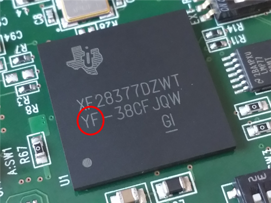
  • As you know, circle section in picture is silicon revision.

    Normally, It marked like 'C', 'CA', 'CB', ...

    What is the meaning of 'YF'?

  • Hello,

    The errata document for the chip should describe this.

    However, I just took a look at it and it is incorrect.  I will submit a bug request to get this fixed once I am back in office.

    The markings on F28M36x chips are similar to the F28377D's markings (see pg 5 of the below).  This should help you understand the markings on the F28377D device.
    http://www.ti.com/lit/er/sprz375c/sprz375c.pdf 

    In short, the YF is 'Wafer Fab Code as Applicable'.


    Thank you,
    Brett

  • I just received a TMS320F28377D Experimenter Kit Friday.  I have been trying to play with the blinky_dc example projects for both CPU1 and CPU2 in controlsuite.  I can load the example project on CPU1 and it runs fine.  I am having trouble loading the blinky_rc example project for CPU2 on the second CPU.  I have not been able to find any step by step instructions on how to work with the two cores of the F28377D.  Is there a document that goes over dealing with two processors in CCS 5.5?  I have done a large amount with the OMAPL138 in CCS and I know there are gel file scripts that allow you to turn on and off the DSP core of the OMAPL138.  I have not been able to find anything similar to that for the F28377D. 

    I am using CCS 5.5 and the latest updates with compile tools 6.2.4 for the 28x series.  I am able to load the CPU1 example and run it.  Then I terminate the CPU1 debug session leaving it running (blinking the LED) and then try to Debug the CPU2 project.  I get the following error when CCS tries to load the program:

    C28xx_CPU2: Breakpoint Manager: Retrying with a AET breakpoint

    C28xx_CPU2: Trouble Setting Breakpoint with the Action "Finish Auto Run" at 0x8148: (Error -1066 @ 0x8148) Unable to set/clear requested breakpoint. Verify that the breakpoint address is in valid memory. (Emulation package 5.1.402.0)

    C28xx_CPU2: Can't Run Target CPU: (Error -1141 @ 0xB78B) Device is not responding to the request. Reset the device, and retry the operation. If error persists, confirm configuration, power-cycle the board, and/or try more reliable JTAG settings (e.g. lower TCLK). (Emulation package 5.1.402.0)

    Any help would be greatly appreciated. 

    Dan

  • Daniel,

    Which build configuration are you using ? 

    I just checked the CPU_RAM_DEBUG setting. I loaded CPU1 first and then CPU2. Then ran CPU1 first followed by CPU2.

    Thanks

    Noah

  • For blinky_dc_cpu1 I am using CPU1_RAM_DEBUG and for blinky_dc_cpu2 I am using CPU2_RAM.

    Could you explain a bit more how from CCS you load CPU1 then load CPU2 then run CPU1 and then run CPU2?  Are you using the Load command or the Debug command under the "Run" menu?  In these steps when does CCS switch to the Debug windows instead of the Edit windows? 

    I have never dealt with loading two processors at the same time.  Thanks for the help.

    Dan


  • Daniel,

    RAM builds of each project should successfully load and run on both CPUs.  Flash builds may have problems with CPU2 (we've had some reports of this that we are investigating).  There is a basic debugging guide for our dual core applications in the firmware examples guide (typically found at C:\ti\controlSUITE\device_support\F2837xD\v100\doc).  There is no way to disable CPUs with GEL files.  If you aren't using a CPU just don't connect to it, or if you are connected just leave it alone.

    The errors you get with CPU2 are due to an error in the memory map definition in the GEL files.  Flash is accidentally marketed as writable so it tries to set a software breakpoint at main (in flash), which isn't possible.  This is a known issue and will be resolved in our next CCS patch.  We are waiting to release this patch until a corresponding emulation patch from Spectrum Digital is released.  This should occur within the next week or so.  Check the sticky posts in our forums for updates.

    BR,

  • Thank you for the help.  I am able to get code running on both cores now.  I will be watching for the patch.

    Dan

  • Hello Chris,

    Too bad it doesn't have any HRCAP modules.  

    PWM down to 55ps - 1 / 55E-12 = 18.18...GHz - really?

    Looks like a nice part - would be great to see a roadmap TI has for improved/new microcontrollers in this family.

    Thanks,
    johnw

  • Dear Chris,

    Can you tell me how many ADC input can be used at maximum with F2837xD?

    Thx

  • This can be found on the product selection table

    http://www.ti.com/lsds/ti/microcontroller/32-bit_c2000/c28x_delfino/products.page

    On the largest package there are 24 dedicated ADC channel pins. This allows for 24 single ended 12-bit channels or 12 differential 16-bit channels.


  • Hi Chris,

    Is it already known when a new revision of datasheet will be released? Some (or most) of electrical specification is missing from the current one. I'm curious for example about the speed specs of SPI modules as you are advertising it's high speed of 40 MHz (i wonder if it is only master transmitter or receiver also).

    Best regards and keep up the good work,

    Andy

  • The next revision of the datasheet will be in the March timeframe.  This revision won't have the electrical data that you are looking for though.  The electricals will be updated later on this year once our internal data is final. 


    Loretta

  • ChrisClearman said:

    This can be found on the product selection table

    http://www.ti.com/lsds/ti/microcontroller/32-bit_c2000/c28x_delfino/products.page

    On the largest package there are 24 dedicated ADC channel pins. This allows for 24 single ended 12-bit channels or 12 differential 16-bit channels.


    Dear Chris,

    I am looking at the datasheet page 73, figure 6-1 which shows ADC structure. ADC-C Block has no ADCINC0 and ADCINC1 pin. So, I am confused whether this controller has 24 or 22 ADC pins.

    Also I see that some inputs of ADC block (6, 7, 10, 11 inputs of ADC blocks) are not tied to any pin or signal in the figure. What is the function of these?

    Thanks

    Thank you

  • Voltage Multiplier,

    Voltage Multiplier said:

    I am looking at the datasheet page 73, figure 6-1 which shows ADC structure. ADC-C Block has no ADCINC0 and ADCINC1 pin. So, I am confused whether this controller has 24 or 22 ADC pins.

    24 ADC inputs = 6 (A0:A5) + 6 (B0:B5) + 2 (Cal0 & Cal1) + 4 (C2:C5) + 6 (D0:D5)


    Voltage Multiplier said:

    Also I see that some inputs of ADC block (6, 7, 10, 11 inputs of ADC blocks) are not tied to any pin or signal in the figure. What is the function of these?

    ADC Inputs 6, 7, 10, 11 (and 0 and 1 on ADC-C) are unused in this device.


    Thank you,
    Brett

  • Loretta Faluade said:

    The next revision of the datasheet will be in the March timeframe.  This revision won't have the electrical data that you are looking for though.  The electricals will be updated later on this year once our internal data is final. 

    Thanks for the update. Can you at least tell me what are the expectations about max. SPI speed in master-receiver mode?

    Regards, Andy

  • Andy,

    The design target is 40MHz but this could be subject to change until we finish characterization. 

    Loretta

  • I have the similar problem too. I received 28377D Kit in Jan. 2014. I also tried the example project blinky_dc. It works but only for built to RAM. Built to FLASH never works. I loaded the .out file to flash. I observed the whole process: erase, program and verify. However, when I checked the flask memory (0x80000, the code entry point), it is blank (all 0xFFs).

    Any idea why? Thanks.


    Keith

  • Hi Chris,

     I'm porting my code to this new device and I would like to add some features as well.

    One of these is the Output X-BAR but I cannot find the " OUTPUTXBARx" pins in the "GPIO Muxed Pins" table while I see the XTRIPOUTx pins of which I cannot find the meaning...are the same thing?

    Thanks a lot.

    Gianluca

  • Keith,

    Have you successfully installed the F28377xD Flash Plug-in? 

    You can read more about the plugin in the following thread:
    http://e2e.ti.com/support/microcontrollers/c2000/f/171/t/314938.aspx


    Thank you,
    Brett

  • Yes, they're the same thing.

    The OUTPUTXBARx pins are labelled "XTRIPOUTx" in the Peripheral Mux table.  Sorry for the confusing wording.

    We'll try to get that cleaned up.

    -Bob

  • Bob,

      thank you very much for your fast reply!

    Gianluca

  • Dear all, 

                  In coming days will there be any "Mat-lab Embedded coder" support for TMS320F2837xD device, as I am into the Model Based design, eagerly waiting for that.


    Kind Regards

    Karuna


  • Dear Karuna,

    MathWorks is actively looking into supporting the TMS320F2837xD devices. These are early investigations though, be prepared to discover support for Concerto before 2837x.

    MathWorks has a policy of not disclosing any support prior to the official release date, for specific questions related to TI C2000 support please email c2000_expert@mathworks.com

    I hope it helps,

    Antonin.