This thread has been locked.
If you have a related question, please click the "Ask a related question" button in the top right corner. The newly created question will be automatically linked to this question.
I have achieved CAN communication successfully on TMS320F28069.
But I need to migrate my code in TMS320F28069 to TMS320F28069M.
Does anyone migrate the code to TMS320F28069M successfully? Can you give me this guidance?Or there are some posts or handbooks as a reference?
it should run immediately.
I guess the challenge is mixing the controlSUITE style code with MotorWare....but just bring in the files used from controlSUITE. I do believe there were some posts on the topic also...
And we do plan to add these drivers/APIs/examples into MotorWare, it's just taking much longer than we would like.
I recently did a port of the ecan driver into an instaspin project. The main key is making sure you include the lines with the #pragma. Once you include the driver, you can basically follow the standard ecan tutorials and documentation from the controlSuite software. You may also need to alter the bit timings depending upon what speed you are running your processor at. I believe this code should work at 500 kpbs though with a clock speed of 90 Mhz.
/* * can.c * * Created on: Jan 7, 2015 * Author: Drew Westrick */ #include "sw/drivers/can/src/32b/f28x/f2806x/ecan.h" #pragma DATA_SECTION(ECanaRegs,"ECanaRegsFile"); volatile struct ECAN_REGS ECanaRegs; #pragma DATA_SECTION(ECanaMboxes,"ECanaMboxesFile"); volatile struct ECAN_MBOXES ECanaMboxes; int Test = 0; void CAN_InitECana(void) // Initialize eCAN-A module { /* Create a shadow register structure for the CAN control registers. This is needed, since only 32-bit access is allowed to these registers. 16-bit access to these registers could potentially corrupt the register contents or return false data. */ struct ECAN_REGS ECanaShadow; asm(" EALLOW"); /* Configure eCAN RX and TX pins for CAN operation using eCAN regs*/ ECanaShadow.CANTIOC.all = ECanaRegs.CANTIOC.all; ECanaShadow.CANTIOC.bit.TXFUNC = 1; ECanaRegs.CANTIOC.all = ECanaShadow.CANTIOC.all; ECanaShadow.CANRIOC.all = ECanaRegs.CANRIOC.all; ECanaShadow.CANRIOC.bit.RXFUNC = 1; ECanaRegs.CANRIOC.all = ECanaShadow.CANRIOC.all; /* Configure eCAN for HECC mode - (reqd to access mailboxes 16 thru 31) */ // HECC mode also enables time-stamping feature ECanaShadow.CANMC.all = ECanaRegs.CANMC.all; ECanaShadow.CANMC.bit.SCB = 1; ECanaRegs.CANMC.all = ECanaShadow.CANMC.all; /* Initialize all bits of 'Message Control Register' to zero */ // Some bits of MSGCTRL register come up in an unknown state. For proper operation, // all bits (including reserved bits) of MSGCTRL must be initialized to zero ECanaMboxes.MBOX0.MSGCTRL.all = 0x00000000; ECanaMboxes.MBOX1.MSGCTRL.all = 0x00000000; ECanaMboxes.MBOX2.MSGCTRL.all = 0x00000000; ECanaMboxes.MBOX3.MSGCTRL.all = 0x00000000; ECanaMboxes.MBOX4.MSGCTRL.all = 0x00000000; ECanaMboxes.MBOX5.MSGCTRL.all = 0x00000000; ECanaMboxes.MBOX6.MSGCTRL.all = 0x00000000; ECanaMboxes.MBOX7.MSGCTRL.all = 0x00000000; ECanaMboxes.MBOX8.MSGCTRL.all = 0x00000000; ECanaMboxes.MBOX9.MSGCTRL.all = 0x00000000; ECanaMboxes.MBOX10.MSGCTRL.all = 0x00000000; ECanaMboxes.MBOX11.MSGCTRL.all = 0x00000000; ECanaMboxes.MBOX12.MSGCTRL.all = 0x00000000; ECanaMboxes.MBOX13.MSGCTRL.all = 0x00000000; ECanaMboxes.MBOX14.MSGCTRL.all = 0x00000000; ECanaMboxes.MBOX15.MSGCTRL.all = 0x00000000; ECanaMboxes.MBOX16.MSGCTRL.all = 0x00000000; ECanaMboxes.MBOX17.MSGCTRL.all = 0x00000000; ECanaMboxes.MBOX18.MSGCTRL.all = 0x00000000; ECanaMboxes.MBOX19.MSGCTRL.all = 0x00000000; ECanaMboxes.MBOX20.MSGCTRL.all = 0x00000000; ECanaMboxes.MBOX21.MSGCTRL.all = 0x00000000; ECanaMboxes.MBOX22.MSGCTRL.all = 0x00000000; ECanaMboxes.MBOX23.MSGCTRL.all = 0x00000000; ECanaMboxes.MBOX24.MSGCTRL.all = 0x00000000; ECanaMboxes.MBOX25.MSGCTRL.all = 0x00000000; ECanaMboxes.MBOX26.MSGCTRL.all = 0x00000000; ECanaMboxes.MBOX27.MSGCTRL.all = 0x00000000; ECanaMboxes.MBOX28.MSGCTRL.all = 0x00000000; ECanaMboxes.MBOX29.MSGCTRL.all = 0x00000000; ECanaMboxes.MBOX30.MSGCTRL.all = 0x00000000; ECanaMboxes.MBOX31.MSGCTRL.all = 0x00000000; // TAn, RMPn, GIFn bits are all zero upon reset and are cleared again // as a matter of precaution. ECanaRegs.CANTA.all = 0xFFFFFFFF; /* Clear all TAn bits */ ECanaRegs.CANRMP.all = 0xFFFFFFFF; /* Clear all RMPn bits */ ECanaRegs.CANGIF0.all = 0xFFFFFFFF; /* Clear all interrupt flag bits */ ECanaRegs.CANGIF1.all = 0xFFFFFFFF; /* Configure bit timing parameters for eCANA*/ ECanaShadow.CANMC.all = ECanaRegs.CANMC.all; ECanaShadow.CANMC.bit.CCR = 1 ; // Set CCR = 1 ECanaRegs.CANMC.all = ECanaShadow.CANMC.all; // Wait until the CPU has been granted permission to change the configuration registers do { ECanaShadow.CANES.all = ECanaRegs.CANES.all; } while(ECanaShadow.CANES.bit.CCE != 1 ); // Wait for CCE bit to be set.. ECanaShadow.CANBTC.all = 0; /* The following block is for 90 MHz SYSCLKOUT. (45 MHz CAN module clock Bit rate = 500 Kbps See Note at end of file. */ ECanaShadow.CANBTC.bit.BRPREG = 8; ECanaShadow.CANBTC.bit.TSEG2REG = 3; ECanaShadow.CANBTC.bit.TSEG1REG = 4; ECanaShadow.CANBTC.bit.SJWREG = 1; ECanaShadow.CANBTC.bit.SAM = 1; ECanaRegs.CANBTC.all = ECanaShadow.CANBTC.all; asm(" EALLOW"); ECanaShadow.CANMC.all = ECanaRegs.CANMC.all; ECanaShadow.CANMC.bit.CCR = 0 ; // Set CCR = 0 ECanaRegs.CANMC.all = ECanaShadow.CANMC.all; // Wait until the CPU no longer has permission to change the configuration registers do { ECanaShadow.CANES.all = ECanaRegs.CANES.all; } while(ECanaShadow.CANES.bit.CCE != 0 ); // Wait for CCE bit to be cleared.. /* Disable all Mailboxes */ ECanaRegs.CANME.all = 0; // Required before writing the MSGIDs asm(" EDIS"); } void CAN_SetupMailboxes(void) { ECanaMboxes.MBOX0.MSGID.bit.STDMSGID = 1; ECanaMboxes.MBOX0.MSGID.bit.IDE = 0; ECanaMboxes.MBOX16.MSGID.bit.STDMSGID = 16; ECanaMboxes.MBOX16.MSGID.bit.IDE = 0; ECanaMboxes.MBOX17.MSGID.bit.STDMSGID = 17; ECanaMboxes.MBOX17.MSGID.bit.IDE = 0; ECanaMboxes.MBOX18.MSGID.bit.STDMSGID = 18; ECanaMboxes.MBOX18.MSGID.bit.IDE = 0; ECanaMboxes.MBOX19.MSGID.bit.STDMSGID = 19; ECanaMboxes.MBOX19.MSGID.bit.IDE = 0; ECanaMboxes.MBOX20.MSGID.bit.STDMSGID = 20; ECanaMboxes.MBOX20.MSGID.bit.IDE = 0; ECanaMboxes.MBOX21.MSGID.bit.STDMSGID = 21; ECanaMboxes.MBOX21.MSGID.bit.IDE = 0; ECanaMboxes.MBOX22.MSGID.bit.STDMSGID = 22; ECanaMboxes.MBOX22.MSGID.bit.IDE = 0; ECanaMboxes.MBOX23.MSGID.bit.STDMSGID = 23; ECanaMboxes.MBOX23.MSGID.bit.IDE = 0; ECanaMboxes.MBOX24.MSGID.bit.STDMSGID = 24; ECanaMboxes.MBOX24.MSGID.bit.IDE = 0; ECanaMboxes.MBOX25.MSGID.bit.STDMSGID = 25; ECanaMboxes.MBOX25.MSGID.bit.IDE = 0; ECanaMboxes.MBOX26.MSGID.bit.STDMSGID = 26; ECanaMboxes.MBOX26.MSGID.bit.IDE = 0; ECanaMboxes.MBOX27.MSGID.bit.STDMSGID = 27; ECanaMboxes.MBOX27.MSGID.bit.IDE = 0; ECanaMboxes.MBOX28.MSGID.bit.STDMSGID = 28; ECanaMboxes.MBOX28.MSGID.bit.IDE = 0; ECanaMboxes.MBOX29.MSGID.bit.STDMSGID = 29; ECanaMboxes.MBOX29.MSGID.bit.IDE = 0; ECanaMboxes.MBOX30.MSGID.bit.STDMSGID = 30; ECanaMboxes.MBOX30.MSGID.bit.IDE = 0; ECanaMboxes.MBOX31.MSGID.bit.STDMSGID = 0; ECanaMboxes.MBOX31.MSGID.bit.IDE = 0; // Configure Mailboxes 0-15 as Tx, 16-31 as Rx // Since this write is to the entire register (instead of a bit // field) a shadow register is not required. ECanaRegs.CANMD.all = 0xFFFF0000; // Enable all Mailboxes */ // Since this write is to the entire register (instead of a bit // field) a shadow register is not required. ECanaRegs.CANME.all = 0xFFFFFFFF; // Specify that 8 bits will be sent/received ECanaMboxes.MBOX0.MSGCTRL.bit.DLC = 8; ECanaMboxes.MBOX16.MSGCTRL.bit.DLC = 8; // Write to the mailbox RAM field of MBOX0 - 15 ECanaMboxes.MBOX0.MDL.all = 0x9555AAA0; ECanaMboxes.MBOX0.MDH.all = 0x89ABCDEF; // Since this write is to the entire register (instead of a bit // field) a shadow register is not required. asm(" EALLOW"); ECanaRegs.CANMIM.all = 0xFFFFFFFF; asm(" EDIS"); } void CAN_CheckRx(void) { struct ECAN_REGS ECanaShadow; if (ECanaRegs.CANRMP.bit.RMP31 == 1) { ECanaShadow.CANRMP.all = ECanaRegs.CANRMP.all; ECanaShadow.CANRMP.bit.RMP31 = 1; ECanaRegs.CANRMP.all = ECanaShadow.CANRMP.all; E2E_Example32b.Byte.BYTE0 = ECanaMboxes.MBOX31.MDL.byte.BYTE0; E2E_Example32b.Byte.BYTE1 = ECanaMboxes.MBOX31.MDL.byte.BYTE1; E2E_Example32b.Byte.BYTE2 = ECanaMboxes.MBOX31.MDL.byte.BYTE2; E2E_Example32b.Byte.BYTE3 = ECanaMboxes.MBOX31.MDL.byte.BYTE3; E2E_Example16b.Byte.BYTE0 = ECanaMboxes.MBOX31.MDH.byte.BYTE4; E2E_Example16b.Byte.BYTE1 = ECanaMboxes.MBOX31.MDH.byte.BYTE5; } }
Drew
Wonderful!!
Thanks for your reply.
I try to migrate the code of "Example_2806xECanBack2Back" to lab01 in motorware.But things are not great,I can not get the returned data in self-test mode and I got two warnings:
I changed it as follows
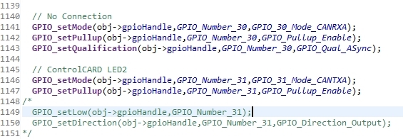
First,I have configure GPIO30 and GPIO31 in hal.c:
// No Connection GPIO_setMode(obj->gpioHandle,GPIO_Number_30,GPIO_30_Mode_CANRXA); // ControlCARD LED2 GPIO_setMode(obj->gpioHandle,GPIO_Number_31,GPIO_31_Mode_CANTXA); /* GPIO_setLow(obj->gpioHandle,GPIO_Number_31); GPIO_setDirection(obj->gpioHandle,GPIO_Number_31,GPIO_Direction_Output); */
Then, I try to migrate the code of "Example_2806xECanBack2Back" to lab01 in motorware
/* --COPYRIGHT--,BSD * Copyright (c) 2012, Texas Instruments Incorporated * All rights reserved. * * Rasm(" EDIS")tribution and use in source and binary forms, with or without * modification, are permitted provided that the following conditions * are met: * * * Rasm(" EDIS")tributions of source code must retain the above copyright * notice, this list of conditions and the following disclaimer. * * * Rasm(" EDIS")tributions in binary form must reproduce the above copyright * notice, this list of conditions and the following disclaimer in the * documentation and/or other materials provided with the distribution. * * * Neither the name of Texas Instruments Incorporated nor the names of * its contributors may be used to endorse or promote products derived * from this software without specific prior written permission. * * THIS SOFTWARE IS PROVIDED BY THE COPYRIGHT HOLDERS AND CONTRIBUTORS "AS IS" * AND ANY EXPRESS OR IMPLIED WARRANTIES, INCLUDING, BUT NOT LIMITED TO, * THE IMPLIED WARRANTIES OF MERCHANTABILITY AND FITNESS FOR A PARTICULAR * PURPOSE ARE DISCLAIMED. IN NO EVENT SHALL THE COPYRIGHT OWNER OR * CONTRIBUTORS BE LIABLE FOR ANY DIRECT, INDIRECT, INCIDENTAL, SPECIAL, * EXEMPLARY, OR CONSEQUENTIAL DAMAGES (INCLUDING, BUT NOT LIMITED TO, * PROCUREMENT OF SUBSTITUTE GOODS OR SERVICES; LOSS OF USE, DATA, OR PROFITS; * OR BUSINESS INTERRUPTION) HOWEVER CAUSED AND ON ANY THEORY OF LIABILITY, * WHETHER IN CONTRACT, STRICT LIABILITY, OR TORT (INCLUDING NEGLIGENCE OR * OTHERWISE) ARISING IN ANY WAY OUT OF THE USE OF THIS SOFTWARE, * EVEN IF ADVISED OF THE POSSIBILITY OF SUCH DAMAGE. * --/COPYRIGHT--*/ //! \file solutions/instaspin_foc/src/proj_lab01.c //! \brief CPU and Inverter Set-up and introduction to interfacing to the ROM library //! //! (C) Copyright 2011, Texas Instruments, Inc. //! \defgroup PROJ_LAB01 PROJ_LAB01 //@{ //! \defgroup PROJ_LAB01_OVERVIEW Project Overview //! //! CPU and Inverter Set-up and introduction to interfacing to the ROM library //! // // ************************************************************************** // the includes // system includes #include <math.h> // modules #include "sw/modules/math/src/32b/math.h" #include "sw/modules/memCopy/src/memCopy.h" #include "sw/drivers/can/src/32b/f28x/f2806x/can.h" #pragma DATA_SECTION(ECanaRegs,"ECanaRegsFile"); volatile struct ECAN_REGS ECanaRegs; #pragma DATA_SECTION(ECanaMboxes,"ECanaMboxesFile"); volatile struct ECAN_MBOXES ECanaMboxes; // drivers // platforms #include "main.h" // ************************************************************************** // the defines #define LED_BLINK_FREQ_Hz 5 // ************************************************************************** // the globals uint_least32_t gLEDcnt = 0; // Counter used to divide down the ISR rate for visually blinking an LED HAL_Handle halHandle; // Handle to the Inverter hardware abstraction layer USER_Params gUserParams; // Contains the user.h settings HAL_PwmData_t gPwmData = {0,0,0}; // Contains PWM duty cycles in global Q format HAL_AdcData_t gAdcData = {0,0,0,0,0,0,0}; // Contains Current and Voltage ADC readings in global Q format volatile MOTOR_Vars_t gMotorVars = MOTOR_Vars_INIT; #ifdef FLASH // Used for running BackGround in flash, and ISR in RAM extern uint_least16_t_t *RamfuncsLoadStart, *RamfuncsLoadEnd, *RamfuncsRunStart; #endif #ifdef DRV8301_SPI // Watch window interface to the 8301 SPI DRV_SPI_8301_Vars_t gDrvSpi8301Vars; #endif uint_least32_t ErrorCount; uint_least32_t PassCount; uint_least32_t MessageReceivedCount; uint_least32_t TestMbox1 = 0; uint_least32_t TestMbox2 = 0; uint_least32_t TestMbox3 = 0; // ************************************************************************** // the functions // Prototype statements for functions found within this file. void mailbox_check(int_least32_t T1, int_least32_t T2, int_least32_t T3); void mailbox_read(int_least16_t i); void InitECana(void); void main(void) { uint_least16_t j; MessageReceivedCount = 0; ErrorCount = 0; PassCount = 0; // eCAN control registers require read/write access using 32-bits. Thus we // will create a set of shadow registers for this example. These shadow // registers will be used to make sure the access is 32-bits and not 16. struct ECAN_REGS ECanaShadow; // Only used if running from FLASH // Note that the variable FLASH is defined by the project #ifdef FLASH // Copy time critical code and Flash setup code to RAM // The RamfuncsLoadStart, RamfuncsLoadEnd, and RamfuncsRunStart // symbols are created by the linker. Refer to the linker files. memCopy((uint_least16_t_t *)&RamfuncsLoadStart,(uint_least16_t_t *)&RamfuncsLoadEnd,(uint_least16_t_t *)&RamfuncsRunStart); #endif // initialize the hardware abstraction layer halHandle = HAL_init(&hal,sizeof(hal)); // check for errors in user parameters USER_checkForErrors(&gUserParams); // store user parameter error in global variable gMotorVars.UserErrorCode = USER_getErrorCode(&gUserParams); // do not allow code execution if there is a user parameter error if(gMotorVars.UserErrorCode != USER_ErrorCode_NoError) { for(;;) { gMotorVars.Flag_enableSys = false; } } // initialize the user parameters USER_setParams(&gUserParams); // set the hardware abstraction layer parameters HAL_setParams(halHandle,&gUserParams); #ifdef LAUNCHPAD // Setup GPIOs 0 and 1 as outputs for use in project lab1 only. // This is specific to the launchpad because its LEDs are also used by the PWM channels. HAL_setupLaunchPadGpio0and1(halHandle); #endif // setup faults HAL_setupFaults(halHandle); // initialize the interrupt vector table HAL_initIntVectorTable(halHandle); // enable the ADC interrupts HAL_enableAdcInts(halHandle); // enable global interrupts HAL_enableGlobalInts(halHandle); // enable debug interrupts HAL_enableDebugInt(halHandle); // disable the PWM HAL_disablePwm(halHandle); #ifdef DRV8301_SPI // turn on the DRV8301 if present HAL_enableDrv(halHandle); // initialize the DRV8301 interface HAL_setupDrvSpi(halHandle,&gDrvSpi8301Vars); #endif InitECana(); // Mailboxs can be written to 16-bits or 32-bits at a time // Write to the MSGID field of TRANSMIT mailboxes MBOX0 - 15 ECanaMboxes.MBOX0.MSGID.all = 0x9555AAA0; ECanaMboxes.MBOX1.MSGID.all = 0x9555AAA1; ECanaMboxes.MBOX2.MSGID.all = 0x9555AAA2; ECanaMboxes.MBOX3.MSGID.all = 0x9555AAA3; ECanaMboxes.MBOX4.MSGID.all = 0x9555AAA4; ECanaMboxes.MBOX5.MSGID.all = 0x9555AAA5; ECanaMboxes.MBOX6.MSGID.all = 0x9555AAA6; ECanaMboxes.MBOX7.MSGID.all = 0x9555AAA7; ECanaMboxes.MBOX8.MSGID.all = 0x9555AAA8; ECanaMboxes.MBOX9.MSGID.all = 0x9555AAA9; ECanaMboxes.MBOX10.MSGID.all = 0x9555AAAA; ECanaMboxes.MBOX11.MSGID.all = 0x9555AAAB; ECanaMboxes.MBOX12.MSGID.all = 0x9555AAAC; ECanaMboxes.MBOX13.MSGID.all = 0x9555AAAD; ECanaMboxes.MBOX14.MSGID.all = 0x9555AAAE; ECanaMboxes.MBOX15.MSGID.all = 0x9555AAAF; // Write to the MSGID field of RECEIVE mailboxes MBOX16 - 31 ECanaMboxes.MBOX16.MSGID.all = 0x9555AAA0; ECanaMboxes.MBOX17.MSGID.all = 0x9555AAA1; ECanaMboxes.MBOX18.MSGID.all = 0x9555AAA2; ECanaMboxes.MBOX19.MSGID.all = 0x9555AAA3; ECanaMboxes.MBOX20.MSGID.all = 0x9555AAA4; ECanaMboxes.MBOX21.MSGID.all = 0x9555AAA5; ECanaMboxes.MBOX22.MSGID.all = 0x9555AAA6; ECanaMboxes.MBOX23.MSGID.all = 0x9555AAA7; ECanaMboxes.MBOX24.MSGID.all = 0x9555AAA8; ECanaMboxes.MBOX25.MSGID.all = 0x9555AAA9; ECanaMboxes.MBOX26.MSGID.all = 0x9555AAAA; ECanaMboxes.MBOX27.MSGID.all = 0x9555AAAB; ECanaMboxes.MBOX28.MSGID.all = 0x9555AAAC; ECanaMboxes.MBOX29.MSGID.all = 0x9555AAAD; ECanaMboxes.MBOX30.MSGID.all = 0x9555AAAE; ECanaMboxes.MBOX31.MSGID.all = 0x9555AAAF; // Configure Mailboxes 0-15 as Tx, 16-31 as Rx // Since this write is to the entire register (instead of a bit // field) a shadow register is not required. ECanaRegs.CANMD.all = 0xFFFF0000; // Enable all Mailboxes */ // Since this write is to the entire register (instead of a bit // field) a shadow register is not required. ECanaRegs.CANME.all = 0xFFFFFFFF; // Specify that 8 bits will be sent/received ECanaMboxes.MBOX0.MSGCTRL.bit.DLC = 8; ECanaMboxes.MBOX1.MSGCTRL.bit.DLC = 8; ECanaMboxes.MBOX2.MSGCTRL.bit.DLC = 8; ECanaMboxes.MBOX3.MSGCTRL.bit.DLC = 8; ECanaMboxes.MBOX4.MSGCTRL.bit.DLC = 8; ECanaMboxes.MBOX5.MSGCTRL.bit.DLC = 8; ECanaMboxes.MBOX6.MSGCTRL.bit.DLC = 8; ECanaMboxes.MBOX7.MSGCTRL.bit.DLC = 8; ECanaMboxes.MBOX8.MSGCTRL.bit.DLC = 8; ECanaMboxes.MBOX9.MSGCTRL.bit.DLC = 8; ECanaMboxes.MBOX10.MSGCTRL.bit.DLC = 8; ECanaMboxes.MBOX11.MSGCTRL.bit.DLC = 8; ECanaMboxes.MBOX12.MSGCTRL.bit.DLC = 8; ECanaMboxes.MBOX13.MSGCTRL.bit.DLC = 8; ECanaMboxes.MBOX14.MSGCTRL.bit.DLC = 8; ECanaMboxes.MBOX15.MSGCTRL.bit.DLC = 8; // Write to the mailbox RAM field of MBOX0 - 15 ECanaMboxes.MBOX0.MDL.all = 0x9555AAA0; ECanaMboxes.MBOX0.MDH.all = 0x89ABCDEF; ECanaMboxes.MBOX1.MDL.all = 0x9555AAA1; ECanaMboxes.MBOX1.MDH.all = 0x89ABCDEF; ECanaMboxes.MBOX2.MDL.all = 0x9555AAA2; ECanaMboxes.MBOX2.MDH.all = 0x89ABCDEF; ECanaMboxes.MBOX3.MDL.all = 0x9555AAA3; ECanaMboxes.MBOX3.MDH.all = 0x89ABCDEF; ECanaMboxes.MBOX4.MDL.all = 0x9555AAA4; ECanaMboxes.MBOX4.MDH.all = 0x89ABCDEF; ECanaMboxes.MBOX5.MDL.all = 0x9555AAA5; ECanaMboxes.MBOX5.MDH.all = 0x89ABCDEF; ECanaMboxes.MBOX6.MDL.all = 0x9555AAA6; ECanaMboxes.MBOX6.MDH.all = 0x89ABCDEF; ECanaMboxes.MBOX7.MDL.all = 0x9555AAA7; ECanaMboxes.MBOX7.MDH.all = 0x89ABCDEF; ECanaMboxes.MBOX8.MDL.all = 0x9555AAA8; ECanaMboxes.MBOX8.MDH.all = 0x89ABCDEF; ECanaMboxes.MBOX9.MDL.all = 0x9555AAA9; ECanaMboxes.MBOX9.MDH.all = 0x89ABCDEF; ECanaMboxes.MBOX10.MDL.all = 0x9555AAAA; ECanaMboxes.MBOX10.MDH.all = 0x89ABCDEF; ECanaMboxes.MBOX11.MDL.all = 0x9555AAAB; ECanaMboxes.MBOX11.MDH.all = 0x89ABCDEF; ECanaMboxes.MBOX12.MDL.all = 0x9555AAAC; ECanaMboxes.MBOX12.MDH.all = 0x89ABCDEF; ECanaMboxes.MBOX13.MDL.all = 0x9555AAAD; ECanaMboxes.MBOX13.MDH.all = 0x89ABCDEF; ECanaMboxes.MBOX14.MDL.all = 0x9555AAAE; ECanaMboxes.MBOX14.MDH.all = 0x89ABCDEF; ECanaMboxes.MBOX15.MDL.all = 0x9555AAAF; ECanaMboxes.MBOX15.MDH.all = 0x89ABCDEF; // Since this write is to the entire register (instead of a bit // field) a shadow register is not required. EALLOW; ECanaRegs.CANMIM.all = 0xFFFFFFFF; // Configure the eCAN for self test mode // Enable the enhanced features of the eCAN. EALLOW; ECanaShadow.CANMC.all = ECanaRegs.CANMC.all; ECanaShadow.CANMC.bit.STM = 1; // Configure CAN for self-test mode ECanaRegs.CANMC.all = ECanaShadow.CANMC.all; EDIS; for(;;) { ECanaRegs.CANTRS.all = 0x0000FFFF; // Set TRS for all transmit mailboxes while(ECanaRegs.CANTA.all != 0x0000FFFF ) {} // Wait for all TAn bits to be set.. ECanaRegs.CANTA.all = 0x0000FFFF; // Clear all TAn MessageReceivedCount++; //Read from Receive mailboxes and begin checking for data */ for(j=16; j<32; j++) // Read & check 16 mailboxes { mailbox_read(j); // This func reads the indicated mailbox data mailbox_check(TestMbox1,TestMbox2,TestMbox3); // Checks the received data } } /* // For ever loop while(true); */ } // end of main() function interrupt void mainISR(void) { // toggle status LED if(gLEDcnt++ > (uint_least32_t)(USER_ISR_FREQ_Hz / LED_BLINK_FREQ_Hz)) { HAL_toggleLed(halHandle,(GPIO_Number_e)HAL_Gpio_LED2); gLEDcnt = 0; } // acknowledge the ADC interrupt HAL_acqAdcInt(halHandle,ADC_IntNumber_1); // convert the ADC data HAL_readAdcData(halHandle,&gAdcData); // ADC processing and pwm result code goes here // write the PWM compare values HAL_writePwmData(halHandle,&gPwmData); return; } // end of mainISR() function // This function reads out the contents of the indicated // by the Mailbox number (MBXnbr). void mailbox_read(int_least16_t MBXnbr) { volatile struct MBOX *Mailbox; Mailbox = &ECanaMboxes.MBOX0 + MBXnbr; TestMbox1 = Mailbox->MDL.all; // = 0x9555AAAn (n is the MBX number) TestMbox2 = Mailbox->MDH.all; // = 0x89ABCDEF (a constant) TestMbox3 = Mailbox->MSGID.all;// = 0x9555AAAn (n is the MBX number) } // MSGID of a rcv MBX is transmitted as the MDL data. void mailbox_check(int_least32_t T1, int_least32_t T2, int_least32_t T3) { if((T1 != T3) || ( T2 != 0x89ABCDEF)) { ErrorCount++; } else { PassCount++; } } void InitECana(void) // Initialize eCAN-A module { /* Create a shadow register structure for the CAN control registers. This is needed, since only 32-bit access is allowed to these registers. 16-bit access to these registers could potentially corrupt the register contents or return false data. */ struct ECAN_REGS ECanaShadow; EALLOW; // asm(" asm(" EALLOW")") enables access to protected bits /* Configure eCAN RX and TX pins for CAN operation using eCAN regs*/ ECanaShadow.CANTIOC.all = ECanaRegs.CANTIOC.all; ECanaShadow.CANTIOC.bit.TXFUNC = 1; ECanaRegs.CANTIOC.all = ECanaShadow.CANTIOC.all; ECanaShadow.CANRIOC.all = ECanaRegs.CANRIOC.all; ECanaShadow.CANRIOC.bit.RXFUNC = 1; ECanaRegs.CANRIOC.all = ECanaShadow.CANRIOC.all; /* Configure eCAN for HECC mode - (reqd to access mailboxes 16 thru 31) */ // HECC mode also enables time-stamping feature ECanaShadow.CANMC.all = ECanaRegs.CANMC.all; ECanaShadow.CANMC.bit.SCB = 1; ECanaRegs.CANMC.all = ECanaShadow.CANMC.all; /* Initialize all bits of 'Message Control Register' to zero */ // Some bits of MSGCTRL register come up in an unknown state. For proper operation, // all bits (including reserved bits) of MSGCTRL must be initialized to zero ECanaMboxes.MBOX0.MSGCTRL.all = 0x00000000; ECanaMboxes.MBOX1.MSGCTRL.all = 0x00000000; ECanaMboxes.MBOX2.MSGCTRL.all = 0x00000000; ECanaMboxes.MBOX3.MSGCTRL.all = 0x00000000; ECanaMboxes.MBOX4.MSGCTRL.all = 0x00000000; ECanaMboxes.MBOX5.MSGCTRL.all = 0x00000000; ECanaMboxes.MBOX6.MSGCTRL.all = 0x00000000; ECanaMboxes.MBOX7.MSGCTRL.all = 0x00000000; ECanaMboxes.MBOX8.MSGCTRL.all = 0x00000000; ECanaMboxes.MBOX9.MSGCTRL.all = 0x00000000; ECanaMboxes.MBOX10.MSGCTRL.all = 0x00000000; ECanaMboxes.MBOX11.MSGCTRL.all = 0x00000000; ECanaMboxes.MBOX12.MSGCTRL.all = 0x00000000; ECanaMboxes.MBOX13.MSGCTRL.all = 0x00000000; ECanaMboxes.MBOX14.MSGCTRL.all = 0x00000000; ECanaMboxes.MBOX15.MSGCTRL.all = 0x00000000; ECanaMboxes.MBOX16.MSGCTRL.all = 0x00000000; ECanaMboxes.MBOX17.MSGCTRL.all = 0x00000000; ECanaMboxes.MBOX18.MSGCTRL.all = 0x00000000; ECanaMboxes.MBOX19.MSGCTRL.all = 0x00000000; ECanaMboxes.MBOX20.MSGCTRL.all = 0x00000000; ECanaMboxes.MBOX21.MSGCTRL.all = 0x00000000; ECanaMboxes.MBOX22.MSGCTRL.all = 0x00000000; ECanaMboxes.MBOX23.MSGCTRL.all = 0x00000000; ECanaMboxes.MBOX24.MSGCTRL.all = 0x00000000; ECanaMboxes.MBOX25.MSGCTRL.all = 0x00000000; ECanaMboxes.MBOX26.MSGCTRL.all = 0x00000000; ECanaMboxes.MBOX27.MSGCTRL.all = 0x00000000; ECanaMboxes.MBOX28.MSGCTRL.all = 0x00000000; ECanaMboxes.MBOX29.MSGCTRL.all = 0x00000000; ECanaMboxes.MBOX30.MSGCTRL.all = 0x00000000; ECanaMboxes.MBOX31.MSGCTRL.all = 0x00000000; // TAn, RMPn, GIFn bits are all zero upon reset and are cleared again // as a matter of precaution. ECanaRegs.CANTA.all = 0xFFFFFFFF; /* Clear all TAn bits */ ECanaRegs.CANRMP.all = 0xFFFFFFFF; /* Clear all RMPn bits */ ECanaRegs.CANGIF0.all = 0xFFFFFFFF; /* Clear all interrupt flag bits */ ECanaRegs.CANGIF1.all = 0xFFFFFFFF; /* Configure bit timing parameters for eCANA*/ ECanaShadow.CANMC.all = ECanaRegs.CANMC.all; ECanaShadow.CANMC.bit.CCR = 1 ; // Set CCR = 1 ECanaRegs.CANMC.all = ECanaShadow.CANMC.all; // Wait until the CPU has been granted permission to change the configuration registers do { ECanaShadow.CANES.all = ECanaRegs.CANES.all; } while(ECanaShadow.CANES.bit.CCE != 1 ); // Wait for CCE bit to be set.. ECanaShadow.CANBTC.all = 0; /* The following block is for 80 MHz SYSCLKOUT. (40 MHz CAN module clock Bit rate = 1 Mbps See Note at end of file. */ ECanaShadow.CANBTC.bit.BRPREG = 1; ECanaShadow.CANBTC.bit.TSEG2REG = 4; ECanaShadow.CANBTC.bit.TSEG1REG = 13; ECanaShadow.CANBTC.bit.SAM = 1; ECanaRegs.CANBTC.all = ECanaShadow.CANBTC.all; ECanaShadow.CANMC.all = ECanaRegs.CANMC.all; ECanaShadow.CANMC.bit.CCR = 0 ; // Set CCR = 0 ECanaRegs.CANMC.all = ECanaShadow.CANMC.all; // Wait until the CPU no longer has permission to change the configuration registers do { ECanaShadow.CANES.all = ECanaRegs.CANES.all; } while(ECanaShadow.CANES.bit.CCE != 0 ); // Wait for CCE bit to be cleared.. /* Disable all Mailboxes */ ECanaRegs.CANME.all = 0; // Required before writing the MSGIDs EDIS; } //@} //defgroup // end of file
I upload my code of lab01 for ecan to see what I miss?
/* --COPYRIGHT--,BSD * Copyright (c) 2012, Texas Instruments Incorporated * All rights reserved. * * Rasm(" EDIS")tribution and use in source and binary forms, with or without * modification, are permitted provided that the following conditions * are met: * * * Rasm(" EDIS")tributions of source code must retain the above copyright * notice, this list of conditions and the following disclaimer. * * * Rasm(" EDIS")tributions in binary form must reproduce the above copyright * notice, this list of conditions and the following disclaimer in the * documentation and/or other materials provided with the distribution. * * * Neither the name of Texas Instruments Incorporated nor the names of * its contributors may be used to endorse or promote products derived * from this software without specific prior written permission. * * THIS SOFTWARE IS PROVIDED BY THE COPYRIGHT HOLDERS AND CONTRIBUTORS "AS IS" * AND ANY EXPRESS OR IMPLIED WARRANTIES, INCLUDING, BUT NOT LIMITED TO, * THE IMPLIED WARRANTIES OF MERCHANTABILITY AND FITNESS FOR A PARTICULAR * PURPOSE ARE DISCLAIMED. IN NO EVENT SHALL THE COPYRIGHT OWNER OR * CONTRIBUTORS BE LIABLE FOR ANY DIRECT, INDIRECT, INCIDENTAL, SPECIAL, * EXEMPLARY, OR CONSEQUENTIAL DAMAGES (INCLUDING, BUT NOT LIMITED TO, * PROCUREMENT OF SUBSTITUTE GOODS OR SERVICES; LOSS OF USE, DATA, OR PROFITS; * OR BUSINESS INTERRUPTION) HOWEVER CAUSED AND ON ANY THEORY OF LIABILITY, * WHETHER IN CONTRACT, STRICT LIABILITY, OR TORT (INCLUDING NEGLIGENCE OR * OTHERWISE) ARISING IN ANY WAY OUT OF THE USE OF THIS SOFTWARE, * EVEN IF ADVISED OF THE POSSIBILITY OF SUCH DAMAGE. * --/COPYRIGHT--*/ //! \file solutions/instaspin_foc/src/proj_lab01.c //! \brief CPU and Inverter Set-up and introduction to interfacing to the ROM library //! //! (C) Copyright 2011, Texas Instruments, Inc. //! \defgroup PROJ_LAB01 PROJ_LAB01 //@{ //! \defgroup PROJ_LAB01_OVERVIEW Project Overview //! //! CPU and Inverter Set-up and introduction to interfacing to the ROM library //! // // ************************************************************************** // the includes // system includes #include <math.h> // modules #include "sw/modules/math/src/32b/math.h" #include "sw/modules/memCopy/src/memCopy.h" #include "sw/drivers/can/src/32b/f28x/f2806x/can.h" #pragma DATA_SECTION(ECanaRegs,"ECanaRegsFile"); volatile struct ECAN_REGS ECanaRegs; #pragma DATA_SECTION(ECanaMboxes,"ECanaMboxesFile"); volatile struct ECAN_MBOXES ECanaMboxes; // drivers // platforms #include "main.h" // ************************************************************************** // the defines #define LED_BLINK_FREQ_Hz 5 // ************************************************************************** // the globals uint_least32_t gLEDcnt = 0; // Counter used to divide down the ISR rate for visually blinking an LED HAL_Handle halHandle; // Handle to the Inverter hardware abstraction layer USER_Params gUserParams; // Contains the user.h settings HAL_PwmData_t gPwmData = {0,0,0}; // Contains PWM duty cycles in global Q format HAL_AdcData_t gAdcData = {0,0,0,0,0,0,0}; // Contains Current and Voltage ADC readings in global Q format volatile MOTOR_Vars_t gMotorVars = MOTOR_Vars_INIT; #ifdef FLASH // Used for running BackGround in flash, and ISR in RAM extern uint_least16_t_t *RamfuncsLoadStart, *RamfuncsLoadEnd, *RamfuncsRunStart; #endif #ifdef DRV8301_SPI // Watch window interface to the 8301 SPI DRV_SPI_8301_Vars_t gDrvSpi8301Vars; #endif uint_least32_t ErrorCount; uint_least32_t PassCount; uint_least32_t MessageReceivedCount; uint_least32_t TestMbox1 = 0; uint_least32_t TestMbox2 = 0; uint_least32_t TestMbox3 = 0; // ************************************************************************** // the functions // Prototype statements for functions found within this file. void mailbox_check(int_least32_t T1, int_least32_t T2, int_least32_t T3); void mailbox_read(int_least16_t i); void InitECana(void); void main(void) { uint_least16_t j; MessageReceivedCount = 0; ErrorCount = 0; PassCount = 0; // eCAN control registers require read/write access using 32-bits. Thus we // will create a set of shadow registers for this example. These shadow // registers will be used to make sure the access is 32-bits and not 16. struct ECAN_REGS ECanaShadow; // Only used if running from FLASH // Note that the variable FLASH is defined by the project #ifdef FLASH // Copy time critical code and Flash setup code to RAM // The RamfuncsLoadStart, RamfuncsLoadEnd, and RamfuncsRunStart // symbols are created by the linker. Refer to the linker files. memCopy((uint_least16_t_t *)&RamfuncsLoadStart,(uint_least16_t_t *)&RamfuncsLoadEnd,(uint_least16_t_t *)&RamfuncsRunStart); #endif // initialize the hardware abstraction layer halHandle = HAL_init(&hal,sizeof(hal)); // check for errors in user parameters USER_checkForErrors(&gUserParams); // store user parameter error in global variable gMotorVars.UserErrorCode = USER_getErrorCode(&gUserParams); // do not allow code execution if there is a user parameter error if(gMotorVars.UserErrorCode != USER_ErrorCode_NoError) { for(;;) { gMotorVars.Flag_enableSys = false; } } // initialize the user parameters USER_setParams(&gUserParams); // set the hardware abstraction layer parameters HAL_setParams(halHandle,&gUserParams); #ifdef LAUNCHPAD // Setup GPIOs 0 and 1 as outputs for use in project lab1 only. // This is specific to the launchpad because its LEDs are also used by the PWM channels. HAL_setupLaunchPadGpio0and1(halHandle); #endif // setup faults HAL_setupFaults(halHandle); // initialize the interrupt vector table HAL_initIntVectorTable(halHandle); // enable the ADC interrupts HAL_enableAdcInts(halHandle); // enable global interrupts HAL_enableGlobalInts(halHandle); // enable debug interrupts HAL_enableDebugInt(halHandle); // disable the PWM HAL_disablePwm(halHandle); #ifdef DRV8301_SPI // turn on the DRV8301 if present HAL_enableDrv(halHandle); // initialize the DRV8301 interface HAL_setupDrvSpi(halHandle,&gDrvSpi8301Vars); #endif InitECana(); // Mailboxs can be written to 16-bits or 32-bits at a time // Write to the MSGID field of TRANSMIT mailboxes MBOX0 - 15 ECanaMboxes.MBOX0.MSGID.all = 0x9555AAA0; ECanaMboxes.MBOX1.MSGID.all = 0x9555AAA1; ECanaMboxes.MBOX2.MSGID.all = 0x9555AAA2; ECanaMboxes.MBOX3.MSGID.all = 0x9555AAA3; ECanaMboxes.MBOX4.MSGID.all = 0x9555AAA4; ECanaMboxes.MBOX5.MSGID.all = 0x9555AAA5; ECanaMboxes.MBOX6.MSGID.all = 0x9555AAA6; ECanaMboxes.MBOX7.MSGID.all = 0x9555AAA7; ECanaMboxes.MBOX8.MSGID.all = 0x9555AAA8; ECanaMboxes.MBOX9.MSGID.all = 0x9555AAA9; ECanaMboxes.MBOX10.MSGID.all = 0x9555AAAA; ECanaMboxes.MBOX11.MSGID.all = 0x9555AAAB; ECanaMboxes.MBOX12.MSGID.all = 0x9555AAAC; ECanaMboxes.MBOX13.MSGID.all = 0x9555AAAD; ECanaMboxes.MBOX14.MSGID.all = 0x9555AAAE; ECanaMboxes.MBOX15.MSGID.all = 0x9555AAAF; // Write to the MSGID field of RECEIVE mailboxes MBOX16 - 31 ECanaMboxes.MBOX16.MSGID.all = 0x9555AAA0; ECanaMboxes.MBOX17.MSGID.all = 0x9555AAA1; ECanaMboxes.MBOX18.MSGID.all = 0x9555AAA2; ECanaMboxes.MBOX19.MSGID.all = 0x9555AAA3; ECanaMboxes.MBOX20.MSGID.all = 0x9555AAA4; ECanaMboxes.MBOX21.MSGID.all = 0x9555AAA5; ECanaMboxes.MBOX22.MSGID.all = 0x9555AAA6; ECanaMboxes.MBOX23.MSGID.all = 0x9555AAA7; ECanaMboxes.MBOX24.MSGID.all = 0x9555AAA8; ECanaMboxes.MBOX25.MSGID.all = 0x9555AAA9; ECanaMboxes.MBOX26.MSGID.all = 0x9555AAAA; ECanaMboxes.MBOX27.MSGID.all = 0x9555AAAB; ECanaMboxes.MBOX28.MSGID.all = 0x9555AAAC; ECanaMboxes.MBOX29.MSGID.all = 0x9555AAAD; ECanaMboxes.MBOX30.MSGID.all = 0x9555AAAE; ECanaMboxes.MBOX31.MSGID.all = 0x9555AAAF; // Configure Mailboxes 0-15 as Tx, 16-31 as Rx // Since this write is to the entire register (instead of a bit // field) a shadow register is not required. ECanaRegs.CANMD.all = 0xFFFF0000; // Enable all Mailboxes */ // Since this write is to the entire register (instead of a bit // field) a shadow register is not required. ECanaRegs.CANME.all = 0xFFFFFFFF; // Specify that 8 bits will be sent/received ECanaMboxes.MBOX0.MSGCTRL.bit.DLC = 8; ECanaMboxes.MBOX1.MSGCTRL.bit.DLC = 8; ECanaMboxes.MBOX2.MSGCTRL.bit.DLC = 8; ECanaMboxes.MBOX3.MSGCTRL.bit.DLC = 8; ECanaMboxes.MBOX4.MSGCTRL.bit.DLC = 8; ECanaMboxes.MBOX5.MSGCTRL.bit.DLC = 8; ECanaMboxes.MBOX6.MSGCTRL.bit.DLC = 8; ECanaMboxes.MBOX7.MSGCTRL.bit.DLC = 8; ECanaMboxes.MBOX8.MSGCTRL.bit.DLC = 8; ECanaMboxes.MBOX9.MSGCTRL.bit.DLC = 8; ECanaMboxes.MBOX10.MSGCTRL.bit.DLC = 8; ECanaMboxes.MBOX11.MSGCTRL.bit.DLC = 8; ECanaMboxes.MBOX12.MSGCTRL.bit.DLC = 8; ECanaMboxes.MBOX13.MSGCTRL.bit.DLC = 8; ECanaMboxes.MBOX14.MSGCTRL.bit.DLC = 8; ECanaMboxes.MBOX15.MSGCTRL.bit.DLC = 8; // Write to the mailbox RAM field of MBOX0 - 15 ECanaMboxes.MBOX0.MDL.all = 0x9555AAA0; ECanaMboxes.MBOX0.MDH.all = 0x89ABCDEF; ECanaMboxes.MBOX1.MDL.all = 0x9555AAA1; ECanaMboxes.MBOX1.MDH.all = 0x89ABCDEF; ECanaMboxes.MBOX2.MDL.all = 0x9555AAA2; ECanaMboxes.MBOX2.MDH.all = 0x89ABCDEF; ECanaMboxes.MBOX3.MDL.all = 0x9555AAA3; ECanaMboxes.MBOX3.MDH.all = 0x89ABCDEF; ECanaMboxes.MBOX4.MDL.all = 0x9555AAA4; ECanaMboxes.MBOX4.MDH.all = 0x89ABCDEF; ECanaMboxes.MBOX5.MDL.all = 0x9555AAA5; ECanaMboxes.MBOX5.MDH.all = 0x89ABCDEF; ECanaMboxes.MBOX6.MDL.all = 0x9555AAA6; ECanaMboxes.MBOX6.MDH.all = 0x89ABCDEF; ECanaMboxes.MBOX7.MDL.all = 0x9555AAA7; ECanaMboxes.MBOX7.MDH.all = 0x89ABCDEF; ECanaMboxes.MBOX8.MDL.all = 0x9555AAA8; ECanaMboxes.MBOX8.MDH.all = 0x89ABCDEF; ECanaMboxes.MBOX9.MDL.all = 0x9555AAA9; ECanaMboxes.MBOX9.MDH.all = 0x89ABCDEF; ECanaMboxes.MBOX10.MDL.all = 0x9555AAAA; ECanaMboxes.MBOX10.MDH.all = 0x89ABCDEF; ECanaMboxes.MBOX11.MDL.all = 0x9555AAAB; ECanaMboxes.MBOX11.MDH.all = 0x89ABCDEF; ECanaMboxes.MBOX12.MDL.all = 0x9555AAAC; ECanaMboxes.MBOX12.MDH.all = 0x89ABCDEF; ECanaMboxes.MBOX13.MDL.all = 0x9555AAAD; ECanaMboxes.MBOX13.MDH.all = 0x89ABCDEF; ECanaMboxes.MBOX14.MDL.all = 0x9555AAAE; ECanaMboxes.MBOX14.MDH.all = 0x89ABCDEF; ECanaMboxes.MBOX15.MDL.all = 0x9555AAAF; ECanaMboxes.MBOX15.MDH.all = 0x89ABCDEF; // Since this write is to the entire register (instead of a bit // field) a shadow register is not required. EALLOW; ECanaRegs.CANMIM.all = 0xFFFFFFFF; // Configure the eCAN for self test mode // Enable the enhanced features of the eCAN. EALLOW; ECanaShadow.CANMC.all = ECanaRegs.CANMC.all; ECanaShadow.CANMC.bit.STM = 1; // Configure CAN for self-test mode ECanaRegs.CANMC.all = ECanaShadow.CANMC.all; EDIS; for(;;) { ECanaRegs.CANTRS.all = 0x0000FFFF; // Set TRS for all transmit mailboxes while(ECanaRegs.CANTA.all != 0x0000FFFF ) {} // Wait for all TAn bits to be set.. ECanaRegs.CANTA.all = 0x0000FFFF; // Clear all TAn MessageReceivedCount++; //Read from Receive mailboxes and begin checking for data */ for(j=16; j<32; j++) // Read & check 16 mailboxes { mailbox_read(j); // This func reads the indicated mailbox data mailbox_check(TestMbox1,TestMbox2,TestMbox3); // Checks the received data } } /* // For ever loop while(true); */ } // end of main() function interrupt void mainISR(void) { // toggle status LED if(gLEDcnt++ > (uint_least32_t)(USER_ISR_FREQ_Hz / LED_BLINK_FREQ_Hz)) { HAL_toggleLed(halHandle,(GPIO_Number_e)HAL_Gpio_LED2); gLEDcnt = 0; } // acknowledge the ADC interrupt HAL_acqAdcInt(halHandle,ADC_IntNumber_1); // convert the ADC data HAL_readAdcData(halHandle,&gAdcData); // ADC processing and pwm result code goes here // write the PWM compare values HAL_writePwmData(halHandle,&gPwmData); return; } // end of mainISR() function // This function reads out the contents of the indicated // by the Mailbox number (MBXnbr). void mailbox_read(int_least16_t MBXnbr) { volatile struct MBOX *Mailbox; Mailbox = &ECanaMboxes.MBOX0 + MBXnbr; TestMbox1 = Mailbox->MDL.all; // = 0x9555AAAn (n is the MBX number) TestMbox2 = Mailbox->MDH.all; // = 0x89ABCDEF (a constant) TestMbox3 = Mailbox->MSGID.all;// = 0x9555AAAn (n is the MBX number) } // MSGID of a rcv MBX is transmitted as the MDL data. void mailbox_check(int_least32_t T1, int_least32_t T2, int_least32_t T3) { if((T1 != T3) || ( T2 != 0x89ABCDEF)) { ErrorCount++; } else { PassCount++; } } void InitECana(void) // Initialize eCAN-A module { /* Create a shadow register structure for the CAN control registers. This is needed, since only 32-bit access is allowed to these registers. 16-bit access to these registers could potentially corrupt the register contents or return false data. */ struct ECAN_REGS ECanaShadow; EALLOW; // asm(" asm(" EALLOW")") enables access to protected bits /* Configure eCAN RX and TX pins for CAN operation using eCAN regs*/ ECanaShadow.CANTIOC.all = ECanaRegs.CANTIOC.all; ECanaShadow.CANTIOC.bit.TXFUNC = 1; ECanaRegs.CANTIOC.all = ECanaShadow.CANTIOC.all; ECanaShadow.CANRIOC.all = ECanaRegs.CANRIOC.all; ECanaShadow.CANRIOC.bit.RXFUNC = 1; ECanaRegs.CANRIOC.all = ECanaShadow.CANRIOC.all; /* Configure eCAN for HECC mode - (reqd to access mailboxes 16 thru 31) */ // HECC mode also enables time-stamping feature ECanaShadow.CANMC.all = ECanaRegs.CANMC.all; ECanaShadow.CANMC.bit.SCB = 1; ECanaRegs.CANMC.all = ECanaShadow.CANMC.all; /* Initialize all bits of 'Message Control Register' to zero */ // Some bits of MSGCTRL register come up in an unknown state. For proper operation, // all bits (including reserved bits) of MSGCTRL must be initialized to zero ECanaMboxes.MBOX0.MSGCTRL.all = 0x00000000; ECanaMboxes.MBOX1.MSGCTRL.all = 0x00000000; ECanaMboxes.MBOX2.MSGCTRL.all = 0x00000000; ECanaMboxes.MBOX3.MSGCTRL.all = 0x00000000; ECanaMboxes.MBOX4.MSGCTRL.all = 0x00000000; ECanaMboxes.MBOX5.MSGCTRL.all = 0x00000000; ECanaMboxes.MBOX6.MSGCTRL.all = 0x00000000; ECanaMboxes.MBOX7.MSGCTRL.all = 0x00000000; ECanaMboxes.MBOX8.MSGCTRL.all = 0x00000000; ECanaMboxes.MBOX9.MSGCTRL.all = 0x00000000; ECanaMboxes.MBOX10.MSGCTRL.all = 0x00000000; ECanaMboxes.MBOX11.MSGCTRL.all = 0x00000000; ECanaMboxes.MBOX12.MSGCTRL.all = 0x00000000; ECanaMboxes.MBOX13.MSGCTRL.all = 0x00000000; ECanaMboxes.MBOX14.MSGCTRL.all = 0x00000000; ECanaMboxes.MBOX15.MSGCTRL.all = 0x00000000; ECanaMboxes.MBOX16.MSGCTRL.all = 0x00000000; ECanaMboxes.MBOX17.MSGCTRL.all = 0x00000000; ECanaMboxes.MBOX18.MSGCTRL.all = 0x00000000; ECanaMboxes.MBOX19.MSGCTRL.all = 0x00000000; ECanaMboxes.MBOX20.MSGCTRL.all = 0x00000000; ECanaMboxes.MBOX21.MSGCTRL.all = 0x00000000; ECanaMboxes.MBOX22.MSGCTRL.all = 0x00000000; ECanaMboxes.MBOX23.MSGCTRL.all = 0x00000000; ECanaMboxes.MBOX24.MSGCTRL.all = 0x00000000; ECanaMboxes.MBOX25.MSGCTRL.all = 0x00000000; ECanaMboxes.MBOX26.MSGCTRL.all = 0x00000000; ECanaMboxes.MBOX27.MSGCTRL.all = 0x00000000; ECanaMboxes.MBOX28.MSGCTRL.all = 0x00000000; ECanaMboxes.MBOX29.MSGCTRL.all = 0x00000000; ECanaMboxes.MBOX30.MSGCTRL.all = 0x00000000; ECanaMboxes.MBOX31.MSGCTRL.all = 0x00000000; // TAn, RMPn, GIFn bits are all zero upon reset and are cleared again // as a matter of precaution. ECanaRegs.CANTA.all = 0xFFFFFFFF; /* Clear all TAn bits */ ECanaRegs.CANRMP.all = 0xFFFFFFFF; /* Clear all RMPn bits */ ECanaRegs.CANGIF0.all = 0xFFFFFFFF; /* Clear all interrupt flag bits */ ECanaRegs.CANGIF1.all = 0xFFFFFFFF; /* Configure bit timing parameters for eCANA*/ ECanaShadow.CANMC.all = ECanaRegs.CANMC.all; ECanaShadow.CANMC.bit.CCR = 1 ; // Set CCR = 1 ECanaRegs.CANMC.all = ECanaShadow.CANMC.all; // Wait until the CPU has been granted permission to change the configuration registers do { ECanaShadow.CANES.all = ECanaRegs.CANES.all; } while(ECanaShadow.CANES.bit.CCE != 1 ); // Wait for CCE bit to be set.. ECanaShadow.CANBTC.all = 0; /* The following block is for 80 MHz SYSCLKOUT. (40 MHz CAN module clock Bit rate = 1 Mbps See Note at end of file. */ ECanaShadow.CANBTC.bit.BRPREG = 1; ECanaShadow.CANBTC.bit.TSEG2REG = 4; ECanaShadow.CANBTC.bit.TSEG1REG = 13; ECanaShadow.CANBTC.bit.SAM = 1; ECanaRegs.CANBTC.all = ECanaShadow.CANBTC.all; ECanaShadow.CANMC.all = ECanaRegs.CANMC.all; ECanaShadow.CANMC.bit.CCR = 0 ; // Set CCR = 0 ECanaRegs.CANMC.all = ECanaShadow.CANMC.all; // Wait until the CPU no longer has permission to change the configuration registers do { ECanaShadow.CANES.all = ECanaRegs.CANES.all; } while(ECanaShadow.CANES.bit.CCE != 0 ); // Wait for CCE bit to be cleared.. /* Disable all Mailboxes */ ECanaRegs.CANME.all = 0; // Required before writing the MSGIDs EDIS; } //@} //defgroup // end of file
chao
Chao,
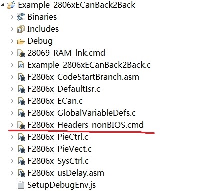
Can you send me a copy of your F2806x_Headers_nonBIOS.cmd file? The Peripheral registers linker command file could be missing a value.
Yes. Try and copy that file over to the pro_lab1 project. I believe the compiler is still having an issue linking the ECANA register to the proper hardware register. If I remember correctly copying that cmd file should fix things. As always let me know how it goes.
Hello Drew
I made a new attempt.
1. In hal.c file,I enable internal pull-up for the selected CAN pins and Set qualification for selected CAN pins to asynch.
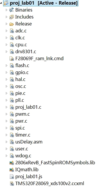
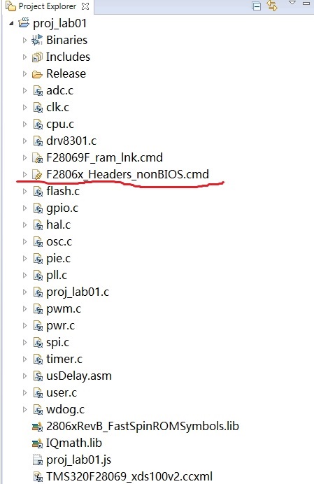
2. I add "F2806x_Headers_nonBIOS.cmd" file into the pro_lab1 project.
After the code was built, I got some advice:
3.I run code and added global variables such as "ErrorCount" "PassCount" " TestMbox1"... into expressions window. They have no changed.
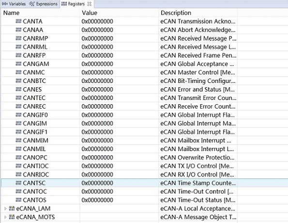
When I saw Register window,I found all the value of registers for ecan were 0.
It meaned that all the register configuration were invalid.I don't have not modified any CMD file.I don't know what I miss.
/* --COPYRIGHT--,BSD * Copyright (c) 2012, Texas Instruments Incorporated * All rights reserved. * * Rasm(" EDIS")tribution and use in source and binary forms, with or without * modification, are permitted provided that the following conditions * are met: * * * Rasm(" EDIS")tributions of source code must retain the above copyright * notice, this list of conditions and the following disclaimer. * * * Rasm(" EDIS")tributions in binary form must reproduce the above copyright * notice, this list of conditions and the following disclaimer in the * documentation and/or other materials provided with the distribution. * * * Neither the name of Texas Instruments Incorporated nor the names of * its contributors may be used to endorse or promote products derived * from this software without specific prior written permission. * * THIS SOFTWARE IS PROVIDED BY THE COPYRIGHT HOLDERS AND CONTRIBUTORS "AS IS" * AND ANY EXPRESS OR IMPLIED WARRANTIES, INCLUDING, BUT NOT LIMITED TO, * THE IMPLIED WARRANTIES OF MERCHANTABILITY AND FITNESS FOR A PARTICULAR * PURPOSE ARE DISCLAIMED. IN NO EVENT SHALL THE COPYRIGHT OWNER OR * CONTRIBUTORS BE LIABLE FOR ANY DIRECT, INDIRECT, INCIDENTAL, SPECIAL, * EXEMPLARY, OR CONSEQUENTIAL DAMAGES (INCLUDING, BUT NOT LIMITED TO, * PROCUREMENT OF SUBSTITUTE GOODS OR SERVICES; LOSS OF USE, DATA, OR PROFITS; * OR BUSINESS INTERRUPTION) HOWEVER CAUSED AND ON ANY THEORY OF LIABILITY, * WHETHER IN CONTRACT, STRICT LIABILITY, OR TORT (INCLUDING NEGLIGENCE OR * OTHERWISE) ARISING IN ANY WAY OUT OF THE USE OF THIS SOFTWARE, * EVEN IF ADVISED OF THE POSSIBILITY OF SUCH DAMAGE. * --/COPYRIGHT--*/ //! \file solutions/instaspin_foc/src/proj_lab01.c //! \brief CPU and Inverter Set-up and introduction to interfacing to the ROM library //! //! (C) Copyright 2011, Texas Instruments, Inc. //! \defgroup PROJ_LAB01 PROJ_LAB01 //@{ //! \defgroup PROJ_LAB01_OVERVIEW Project Overview //! //! CPU and Inverter Set-up and introduction to interfacing to the ROM library //! // // ************************************************************************** // the includes // system includes #include <math.h> // modules #include "sw/modules/math/src/32b/math.h" #include "sw/modules/memCopy/src/memCopy.h" #include "sw/drivers/can/src/32b/f28x/f2806x/can.h" #pragma DATA_SECTION(ECanaRegs,"ECanaRegsFile"); volatile struct ECAN_REGS ECanaRegs; #pragma DATA_SECTION(ECanaMboxes,"ECanaMboxesFile"); volatile struct ECAN_MBOXES ECanaMboxes; // drivers // platforms #include "main.h" // ************************************************************************** // the defines #define LED_BLINK_FREQ_Hz 5 // ************************************************************************** // the globals uint_least32_t gLEDcnt = 0; // Counter used to divide down the ISR rate for visually blinking an LED HAL_Handle halHandle; // Handle to the Inverter hardware abstraction layer USER_Params gUserParams; // Contains the user.h settings HAL_PwmData_t gPwmData = {0,0,0}; // Contains PWM duty cycles in global Q format HAL_AdcData_t gAdcData = {0,0,0,0,0,0,0}; // Contains Current and Voltage ADC readings in global Q format volatile MOTOR_Vars_t gMotorVars = MOTOR_Vars_INIT; #ifdef FLASH // Used for running BackGround in flash, and ISR in RAM extern uint_least16_t_t *RamfuncsLoadStart, *RamfuncsLoadEnd, *RamfuncsRunStart; #endif #ifdef DRV8301_SPI // Watch window interface to the 8301 SPI DRV_SPI_8301_Vars_t gDrvSpi8301Vars; #endif uint_least32_t ErrorCount; uint_least32_t PassCount; uint_least32_t MessageReceivedCount; uint_least32_t TestMbox1 = 0; uint_least32_t TestMbox2 = 0; uint_least32_t TestMbox3 = 0; // ************************************************************************** // the functions // Prototype statements for functions found within this file. void mailbox_check(int_least32_t T1, int_least32_t T2, int_least32_t T3); void mailbox_read(int_least16_t i); void InitECana(void); void main(void) { uint_least16_t j; MessageReceivedCount = 0; ErrorCount = 0; PassCount = 0; // eCAN control registers require read/write access using 32-bits. Thus we // will create a set of shadow registers for this example. These shadow // registers will be used to make sure the access is 32-bits and not 16. struct ECAN_REGS ECanaShadow; // Only used if running from FLASH // Note that the variable FLASH is defined by the project #ifdef FLASH // Copy time critical code and Flash setup code to RAM // The RamfuncsLoadStart, RamfuncsLoadEnd, and RamfuncsRunStart // symbols are created by the linker. Refer to the linker files. memCopy((uint_least16_t_t *)&RamfuncsLoadStart,(uint_least16_t_t *)&RamfuncsLoadEnd,(uint_least16_t_t *)&RamfuncsRunStart); #endif // initialize the hardware abstraction layer halHandle = HAL_init(&hal,sizeof(hal)); // check for errors in user parameters USER_checkForErrors(&gUserParams); // store user parameter error in global variable gMotorVars.UserErrorCode = USER_getErrorCode(&gUserParams); // do not allow code execution if there is a user parameter error if(gMotorVars.UserErrorCode != USER_ErrorCode_NoError) { for(;;) { gMotorVars.Flag_enableSys = false; } } // initialize the user parameters USER_setParams(&gUserParams); // set the hardware abstraction layer parameters HAL_setParams(halHandle,&gUserParams); #ifdef LAUNCHPAD // Setup GPIOs 0 and 1 as outputs for use in project lab1 only. // This is specific to the launchpad because its LEDs are also used by the PWM channels. HAL_setupLaunchPadGpio0and1(halHandle); #endif // setup faults HAL_setupFaults(halHandle); // initialize the interrupt vector table HAL_initIntVectorTable(halHandle); // enable the ADC interrupts HAL_enableAdcInts(halHandle); // enable global interrupts HAL_enableGlobalInts(halHandle); // enable debug interrupts HAL_enableDebugInt(halHandle); // disable the PWM HAL_disablePwm(halHandle); #ifdef DRV8301_SPI // turn on the DRV8301 if present HAL_enableDrv(halHandle); // initialize the DRV8301 interface HAL_setupDrvSpi(halHandle,&gDrvSpi8301Vars); #endif InitECana(); // Mailboxs can be written to 16-bits or 32-bits at a time // Write to the MSGID field of TRANSMIT mailboxes MBOX0 - 15 ECanaMboxes.MBOX0.MSGID.all = 0x9555AAA0; ECanaMboxes.MBOX1.MSGID.all = 0x9555AAA1; ECanaMboxes.MBOX2.MSGID.all = 0x9555AAA2; ECanaMboxes.MBOX3.MSGID.all = 0x9555AAA3; ECanaMboxes.MBOX4.MSGID.all = 0x9555AAA4; ECanaMboxes.MBOX5.MSGID.all = 0x9555AAA5; ECanaMboxes.MBOX6.MSGID.all = 0x9555AAA6; ECanaMboxes.MBOX7.MSGID.all = 0x9555AAA7; ECanaMboxes.MBOX8.MSGID.all = 0x9555AAA8; ECanaMboxes.MBOX9.MSGID.all = 0x9555AAA9; ECanaMboxes.MBOX10.MSGID.all = 0x9555AAAA; ECanaMboxes.MBOX11.MSGID.all = 0x9555AAAB; ECanaMboxes.MBOX12.MSGID.all = 0x9555AAAC; ECanaMboxes.MBOX13.MSGID.all = 0x9555AAAD; ECanaMboxes.MBOX14.MSGID.all = 0x9555AAAE; ECanaMboxes.MBOX15.MSGID.all = 0x9555AAAF; // Write to the MSGID field of RECEIVE mailboxes MBOX16 - 31 ECanaMboxes.MBOX16.MSGID.all = 0x9555AAA0; ECanaMboxes.MBOX17.MSGID.all = 0x9555AAA1; ECanaMboxes.MBOX18.MSGID.all = 0x9555AAA2; ECanaMboxes.MBOX19.MSGID.all = 0x9555AAA3; ECanaMboxes.MBOX20.MSGID.all = 0x9555AAA4; ECanaMboxes.MBOX21.MSGID.all = 0x9555AAA5; ECanaMboxes.MBOX22.MSGID.all = 0x9555AAA6; ECanaMboxes.MBOX23.MSGID.all = 0x9555AAA7; ECanaMboxes.MBOX24.MSGID.all = 0x9555AAA8; ECanaMboxes.MBOX25.MSGID.all = 0x9555AAA9; ECanaMboxes.MBOX26.MSGID.all = 0x9555AAAA; ECanaMboxes.MBOX27.MSGID.all = 0x9555AAAB; ECanaMboxes.MBOX28.MSGID.all = 0x9555AAAC; ECanaMboxes.MBOX29.MSGID.all = 0x9555AAAD; ECanaMboxes.MBOX30.MSGID.all = 0x9555AAAE; ECanaMboxes.MBOX31.MSGID.all = 0x9555AAAF; // Configure Mailboxes 0-15 as Tx, 16-31 as Rx // Since this write is to the entire register (instead of a bit // field) a shadow register is not required. ECanaRegs.CANMD.all = 0xFFFF0000; // Enable all Mailboxes */ // Since this write is to the entire register (instead of a bit // field) a shadow register is not required. ECanaRegs.CANME.all = 0xFFFFFFFF; // Specify that 8 bits will be sent/received ECanaMboxes.MBOX0.MSGCTRL.bit.DLC = 8; ECanaMboxes.MBOX1.MSGCTRL.bit.DLC = 8; ECanaMboxes.MBOX2.MSGCTRL.bit.DLC = 8; ECanaMboxes.MBOX3.MSGCTRL.bit.DLC = 8; ECanaMboxes.MBOX4.MSGCTRL.bit.DLC = 8; ECanaMboxes.MBOX5.MSGCTRL.bit.DLC = 8; ECanaMboxes.MBOX6.MSGCTRL.bit.DLC = 8; ECanaMboxes.MBOX7.MSGCTRL.bit.DLC = 8; ECanaMboxes.MBOX8.MSGCTRL.bit.DLC = 8; ECanaMboxes.MBOX9.MSGCTRL.bit.DLC = 8; ECanaMboxes.MBOX10.MSGCTRL.bit.DLC = 8; ECanaMboxes.MBOX11.MSGCTRL.bit.DLC = 8; ECanaMboxes.MBOX12.MSGCTRL.bit.DLC = 8; ECanaMboxes.MBOX13.MSGCTRL.bit.DLC = 8; ECanaMboxes.MBOX14.MSGCTRL.bit.DLC = 8; ECanaMboxes.MBOX15.MSGCTRL.bit.DLC = 8; // Write to the mailbox RAM field of MBOX0 - 15 ECanaMboxes.MBOX0.MDL.all = 0x9555AAA0; ECanaMboxes.MBOX0.MDH.all = 0x89ABCDEF; ECanaMboxes.MBOX1.MDL.all = 0x9555AAA1; ECanaMboxes.MBOX1.MDH.all = 0x89ABCDEF; ECanaMboxes.MBOX2.MDL.all = 0x9555AAA2; ECanaMboxes.MBOX2.MDH.all = 0x89ABCDEF; ECanaMboxes.MBOX3.MDL.all = 0x9555AAA3; ECanaMboxes.MBOX3.MDH.all = 0x89ABCDEF; ECanaMboxes.MBOX4.MDL.all = 0x9555AAA4; ECanaMboxes.MBOX4.MDH.all = 0x89ABCDEF; ECanaMboxes.MBOX5.MDL.all = 0x9555AAA5; ECanaMboxes.MBOX5.MDH.all = 0x89ABCDEF; ECanaMboxes.MBOX6.MDL.all = 0x9555AAA6; ECanaMboxes.MBOX6.MDH.all = 0x89ABCDEF; ECanaMboxes.MBOX7.MDL.all = 0x9555AAA7; ECanaMboxes.MBOX7.MDH.all = 0x89ABCDEF; ECanaMboxes.MBOX8.MDL.all = 0x9555AAA8; ECanaMboxes.MBOX8.MDH.all = 0x89ABCDEF; ECanaMboxes.MBOX9.MDL.all = 0x9555AAA9; ECanaMboxes.MBOX9.MDH.all = 0x89ABCDEF; ECanaMboxes.MBOX10.MDL.all = 0x9555AAAA; ECanaMboxes.MBOX10.MDH.all = 0x89ABCDEF; ECanaMboxes.MBOX11.MDL.all = 0x9555AAAB; ECanaMboxes.MBOX11.MDH.all = 0x89ABCDEF; ECanaMboxes.MBOX12.MDL.all = 0x9555AAAC; ECanaMboxes.MBOX12.MDH.all = 0x89ABCDEF; ECanaMboxes.MBOX13.MDL.all = 0x9555AAAD; ECanaMboxes.MBOX13.MDH.all = 0x89ABCDEF; ECanaMboxes.MBOX14.MDL.all = 0x9555AAAE; ECanaMboxes.MBOX14.MDH.all = 0x89ABCDEF; ECanaMboxes.MBOX15.MDL.all = 0x9555AAAF; ECanaMboxes.MBOX15.MDH.all = 0x89ABCDEF; // Since this write is to the entire register (instead of a bit // field) a shadow register is not required. EALLOW; ECanaRegs.CANMIM.all = 0xFFFFFFFF; // Configure the eCAN for self test mode // Enable the enhanced features of the eCAN. EALLOW; ECanaShadow.CANMC.all = ECanaRegs.CANMC.all; ECanaShadow.CANMC.bit.STM = 1; // Configure CAN for self-test mode ECanaRegs.CANMC.all = ECanaShadow.CANMC.all; EDIS; for(;;) { ECanaRegs.CANTRS.all = 0x0000FFFF; // Set TRS for all transmit mailboxes while(ECanaRegs.CANTA.all != 0x0000FFFF ) {} // Wait for all TAn bits to be set.. ECanaRegs.CANTA.all = 0x0000FFFF; // Clear all TAn MessageReceivedCount++; //Read from Receive mailboxes and begin checking for data */ for(j=16; j<32; j++) // Read & check 16 mailboxes { mailbox_read(j); // This func reads the indicated mailbox data mailbox_check(TestMbox1,TestMbox2,TestMbox3); // Checks the received data } } /* // For ever loop while(true); */ } // end of main() function interrupt void mainISR(void) { /* // toggle status LED if(gLEDcnt++ > (uint_least32_t)(USER_ISR_FREQ_Hz / LED_BLINK_FREQ_Hz)) { HAL_toggleLed(halHandle,(GPIO_Number_e)HAL_Gpio_LED2); gLEDcnt = 0; } */ // acknowledge the ADC interrupt HAL_acqAdcInt(halHandle,ADC_IntNumber_1); // convert the ADC data HAL_readAdcData(halHandle,&gAdcData); // ADC processing and pwm result code goes here // write the PWM compare values HAL_writePwmData(halHandle,&gPwmData); return; } // end of mainISR() function // This function reads out the contents of the indicated // by the Mailbox number (MBXnbr). void mailbox_read(int_least16_t MBXnbr) { volatile struct MBOX *Mailbox; Mailbox = &ECanaMboxes.MBOX0 + MBXnbr; TestMbox1 = Mailbox->MDL.all; // = 0x9555AAAn (n is the MBX number) TestMbox2 = Mailbox->MDH.all; // = 0x89ABCDEF (a constant) TestMbox3 = Mailbox->MSGID.all;// = 0x9555AAAn (n is the MBX number) } // MSGID of a rcv MBX is transmitted as the MDL data. void mailbox_check(int_least32_t T1, int_least32_t T2, int_least32_t T3) { if((T1 != T3) || ( T2 != 0x89ABCDEF)) { ErrorCount++; } else { PassCount++; } } void InitECana(void) // Initialize eCAN-A module { /* Create a shadow register structure for the CAN control registers. This is needed, since only 32-bit access is allowed to these registers. 16-bit access to these registers could potentially corrupt the register contents or return false data. */ struct ECAN_REGS ECanaShadow; EALLOW; // EALLOW enables access to protected bits /* Configure eCAN RX and TX pins for CAN operation using eCAN regs*/ ECanaShadow.CANTIOC.all = ECanaRegs.CANTIOC.all; ECanaShadow.CANTIOC.bit.TXFUNC = 1; ECanaRegs.CANTIOC.all = ECanaShadow.CANTIOC.all; ECanaShadow.CANRIOC.all = ECanaRegs.CANRIOC.all; ECanaShadow.CANRIOC.bit.RXFUNC = 1; ECanaRegs.CANRIOC.all = ECanaShadow.CANRIOC.all; /* Configure eCAN for HECC mode - (reqd to access mailboxes 16 thru 31) */ // HECC mode also enables time-stamping feature ECanaShadow.CANMC.all = ECanaRegs.CANMC.all; ECanaShadow.CANMC.bit.SCB = 1; ECanaRegs.CANMC.all = ECanaShadow.CANMC.all; /* Initialize all bits of 'Message Control Register' to zero */ // Some bits of MSGCTRL register come up in an unknown state. For proper operation, // all bits (including reserved bits) of MSGCTRL must be initialized to zero ECanaMboxes.MBOX0.MSGCTRL.all = 0x00000000; ECanaMboxes.MBOX1.MSGCTRL.all = 0x00000000; ECanaMboxes.MBOX2.MSGCTRL.all = 0x00000000; ECanaMboxes.MBOX3.MSGCTRL.all = 0x00000000; ECanaMboxes.MBOX4.MSGCTRL.all = 0x00000000; ECanaMboxes.MBOX5.MSGCTRL.all = 0x00000000; ECanaMboxes.MBOX6.MSGCTRL.all = 0x00000000; ECanaMboxes.MBOX7.MSGCTRL.all = 0x00000000; ECanaMboxes.MBOX8.MSGCTRL.all = 0x00000000; ECanaMboxes.MBOX9.MSGCTRL.all = 0x00000000; ECanaMboxes.MBOX10.MSGCTRL.all = 0x00000000; ECanaMboxes.MBOX11.MSGCTRL.all = 0x00000000; ECanaMboxes.MBOX12.MSGCTRL.all = 0x00000000; ECanaMboxes.MBOX13.MSGCTRL.all = 0x00000000; ECanaMboxes.MBOX14.MSGCTRL.all = 0x00000000; ECanaMboxes.MBOX15.MSGCTRL.all = 0x00000000; ECanaMboxes.MBOX16.MSGCTRL.all = 0x00000000; ECanaMboxes.MBOX17.MSGCTRL.all = 0x00000000; ECanaMboxes.MBOX18.MSGCTRL.all = 0x00000000; ECanaMboxes.MBOX19.MSGCTRL.all = 0x00000000; ECanaMboxes.MBOX20.MSGCTRL.all = 0x00000000; ECanaMboxes.MBOX21.MSGCTRL.all = 0x00000000; ECanaMboxes.MBOX22.MSGCTRL.all = 0x00000000; ECanaMboxes.MBOX23.MSGCTRL.all = 0x00000000; ECanaMboxes.MBOX24.MSGCTRL.all = 0x00000000; ECanaMboxes.MBOX25.MSGCTRL.all = 0x00000000; ECanaMboxes.MBOX26.MSGCTRL.all = 0x00000000; ECanaMboxes.MBOX27.MSGCTRL.all = 0x00000000; ECanaMboxes.MBOX28.MSGCTRL.all = 0x00000000; ECanaMboxes.MBOX29.MSGCTRL.all = 0x00000000; ECanaMboxes.MBOX30.MSGCTRL.all = 0x00000000; ECanaMboxes.MBOX31.MSGCTRL.all = 0x00000000; // TAn, RMPn, GIFn bits are all zero upon reset and are cleared again // as a matter of precaution. ECanaRegs.CANTA.all = 0xFFFFFFFF; /* Clear all TAn bits */ ECanaRegs.CANRMP.all = 0xFFFFFFFF; /* Clear all RMPn bits */ ECanaRegs.CANGIF0.all = 0xFFFFFFFF; /* Clear all interrupt flag bits */ ECanaRegs.CANGIF1.all = 0xFFFFFFFF; /* Configure bit timing parameters for eCANA*/ ECanaShadow.CANMC.all = ECanaRegs.CANMC.all; ECanaShadow.CANMC.bit.CCR = 1 ; // Set CCR = 1 ECanaRegs.CANMC.all = ECanaShadow.CANMC.all; // Wait until the CPU has been granted permission to change the configuration registers do { ECanaShadow.CANES.all = ECanaRegs.CANES.all; } while(ECanaShadow.CANES.bit.CCE != 1 ); // Wait for CCE bit to be set.. ECanaShadow.CANBTC.all = 0; /* The following block is for 80 MHz SYSCLKOUT. (40 MHz CAN module clock Bit rate = 1 Mbps See Note at end of file. */ ECanaShadow.CANBTC.bit.BRPREG = 8; ECanaShadow.CANBTC.bit.TSEG2REG = 3; ECanaShadow.CANBTC.bit.TSEG1REG = 4; ECanaShadow.CANBTC.bit.SAM = 1; ECanaRegs.CANBTC.all = ECanaShadow.CANBTC.all; ECanaShadow.CANMC.all = ECanaRegs.CANMC.all; ECanaShadow.CANMC.bit.CCR = 0 ; // Set CCR = 0 ECanaRegs.CANMC.all = ECanaShadow.CANMC.all; // Wait until the CPU no longer has permission to change the configuration registers do { ECanaShadow.CANES.all = ECanaRegs.CANES.all; } while(ECanaShadow.CANES.bit.CCE != 0 ); // Wait for CCE bit to be cleared.. /* Disable all Mailboxes */ ECanaRegs.CANME.all = 0; // Required before writing the MSGIDs EDIS; } //@} //defgroup // end of file
Hello
I am trying to do exactly the same thing and my program is hanging in exactly the same line of code. In the beginning I thought that it could be due to the the CAN clock not being set properly but I have looked through it in detail and I think that is not the issue. Anyone has been able so solve it?
Hi,
I'm having the same problem and doing the steps described above didn't solve the problem.
I'm using the lab12b as reference to my project.
I have included the F2806x_Headers_nonBIOS.cmd (it was already with the corrections that Javier did) and the project now has two .cmd files.
I can compile without problems or advices, but when I run it, the CCE bit did not change all the time.
// Wait until the CPU has been granted permission to change the configuration registers
do
{
ECanaShadow.CANES.all = ECanaRegs.CANES.all;
} while(ECanaShadow.CANES.bit.CCE != 1 ); // Wait for CCE bit to be set..
I don't Know what is wrong or missing.
I am sorry.No progress.I have yet to work out a way to solve the problem.I think a lot of customer will encounter this problem.I hope TI can give some ways.
Nope still studying the problem. I have made several attempts, different approachs, but no luck yet. I have begun studying the CAN registers in the real time emulator mode. I have successful CAN transfer on the F28335 but no luck on the F28069. I still see no reason why code for the F28069 shouldn't work for the F28069M except for base clock speed. I just stumbled upon a conflict in ssqc019, lab 11, page 11-29, figure 11-44. Compared to TMS320x2806x Piccolo Technical Reference Manual, spruh18e, page page 1066, bit-timing configuration register. One reference states that the calculation for TQ (Time Quantum) is SYSCLKOUT/2 while the other states it's just SYSCLKOUT. The reference manual is probably the right one. The controlCARD F28069M is a 20 MHz clock. If you want me to try you code out for the F28069, I'll give it a whack.
Kurt
Chao,
From a CAN perspective, 28069 or 28069M devices should behave in an identical fashion. The eCAN IP in all 28xx devices are identical (ignoring minor differences external to the module, such as input clock frequency for the module etc). Reading through the thread, it appears code is getting stuck waiting for CCE bit to become 1, is this correct? What is the status of the CANRX pin (or the bus)? Is the bus idle?
Some progress. First I want LED3 to blink so I'll know the mainISR loop is working:
// toggle status //LED2 & LED3
if(gLEDcnt++ > (uint_least32_t)(USER_ISR_FREQ_Hz / LED_BLINK_FREQ_Hz))
{
// HAL_toggleLed(halHandle,(GPIO_Number_e)HAL_Gpio_LED2);// both LED's can blink
HAL_toggleLed(halHandle,(GPIO_Number_e)HAL_Gpio_LED3);
gLEDcnt = 0;
}
and use your GPIO modification in file "hal.c" which allows GPIO31 for CAN TX
Next, in "hal.c" I add the function:
void HAL_setupPeripheralClks2(HAL_Handle handle)
{
HAL_Obj *obj = (HAL_Obj *)handle;
CLK_enableEcanaClock(obj->clkHandle);
return;
} // end of HAL_setupPeripheralClks2() function
and in "hal.h":
//! \brief Sets up the peripheral clocks
//! \param[in] handle The hardware abstraction layer (HAL) handle
extern void HAL_setupPeripheralClks(HAL_Handle handle); // disables eCAN clock
extern void HAL_setupPeripheralClks2(HAL_Handle handle); // enables eCAN clock
I can now add the entire "void InitECana(void)" function at the bottom of proj_lab01.c and add the following two lines before the forever loop in main():
HAL_setupPeripheralClks2(halHandle);
InitECana();
// For ever loop
while(true);
Now I run it on an F28069M controlCARD mounted in a DRV8301 controller board and the PCLKCR0 register is set to x470C and the eCAN time stamp clock is running and the CANTBC register has been set.
Yes. F28069M CAN on DRV8301 board working. If you read my previous posting, the CAN clock has to be enabled. The next significant detail occurs on page 1051, spruh18e.pdf, under the section "16.5.3 CAN Module Operation in Normal Configuration". The TX/RX CAN node must be connected to a second CAN TX/RX node in order for the acknowledge mechanism to function. Then I just commented out the self test mode lines, connected it to a working F28335 TX/RX pair (Lab11 1&2), connected a scope for viewing and it's working. Thanks to Veikko Immonen for programming various tips. The CAN program snippet immediately after the entry into the forever loop (from Chao Yang) was copied into the "while(!(gMotorVars.Flag_enableSys))" loop.
SUMMARY: F28069M/DRV8301 InstaSPIN project 2a lab was grafted with 280xECanBack2Back and connected to a F28335 CAN Lab 11 TX/RX node-pair@100kbps. Functionality was demonstrated by observing CAN signals through an oscilloscope and by placing the InstaSPIN proj02a in Enable_System and Run_Identify modes.
File references:
//! \file solutions/instaspin_foc/src/proj_lab02a.c
//! \brief Using InstaSPIN™-FOC for the first time, Motor ID, full control system from ROM
//! (C) Copyright 2011, Texas Instruments, Inc.
// Checkin $Date: December 3, 2004 13:58:42 $
//###########################################################################
// FILE: Example_280xECanBack2Back.c
// TITLE: DSP280x eCAN Back-to-back transmission and reception in
// SELF-TEST mode
Comment on final header:
// Working2_proj_lab02a_in_proj01_chaoyang
// modified by Kurt J. Kloesel 12/7/2015
// Enable_Sys and Run_Identify_Sys
// This program and hardware must be connected to another CAN node to work
// This program will default into writing and reading mailboxes 0-15 and 16-32
// when connected to a F28335 100kbps systems (Lab11 1_TX and 2R_X)
// 1.) State 0 - writing and reading MessageCount increasing
// 2.) State 1 - Enable_Sys = 1 not CAN TX/RX from F28069 board
// 3.) State 2 - Run_Identify = 1 not CAN TX/RX from F28069 board. but running and identifying motor
// 4.) Return - Enable_Sys=0 & Run_Identify=0 CAN TX/RX from F28069 board working
// Therefore this program demonstrates the "while(!(gMotorVars.Flag_enableSys))" state with F28069 CAN TX/RX
// and transitions into motor identification states
//
Sowmya,
Motorware now includes a proper can.h file in the driver directory located at: \sw\drivers\can\src\32b\f28x\f2806x\. I would start by including that in your project. The next step would be to look at the code in: ti\controlSUITE\device_support\f2806x\v151\F2806x_examples_ccsv5\ecan_back2back. This should provide you with an example of how to use the CAN module to transmit and receive code. I wish there was a nice plug and play middleware CAN driver I could point you towards, but I've always ended up having to write my own for these types of projects. I would give you the code I last wrote for CAN and instaspin, but I doubt it would work with the newer versions of motorware since I took a lot of the header files from the controlSUITE library and grafted them into my motorware project.
Good Luck,
Hi Drew,
My query is moved to a newer thread by TI support. Here is the link - e2e.ti.com/.../614448.
As for this thread , though a deviation, I was wondering if I can get any tips on what registers to mainly change to move from self test mode to normal mode operation. I am assuming the Shadow register is no longer needed. This I'd like to first test only the Launchpad with C2000 ware base , before I move on to motorware.
Do you have code to do this?
Its probably better if I get the basic functionality working before I move on to configuring the HAL object.
Sowmya