This thread has been locked.

If you have a related question, please click the "Ask a related question" button in the top right corner. The newly created question will be automatically linked to this question.

ADC REF with REF3030 LDO

Other Parts Discussed in Thread: REF3030

hi

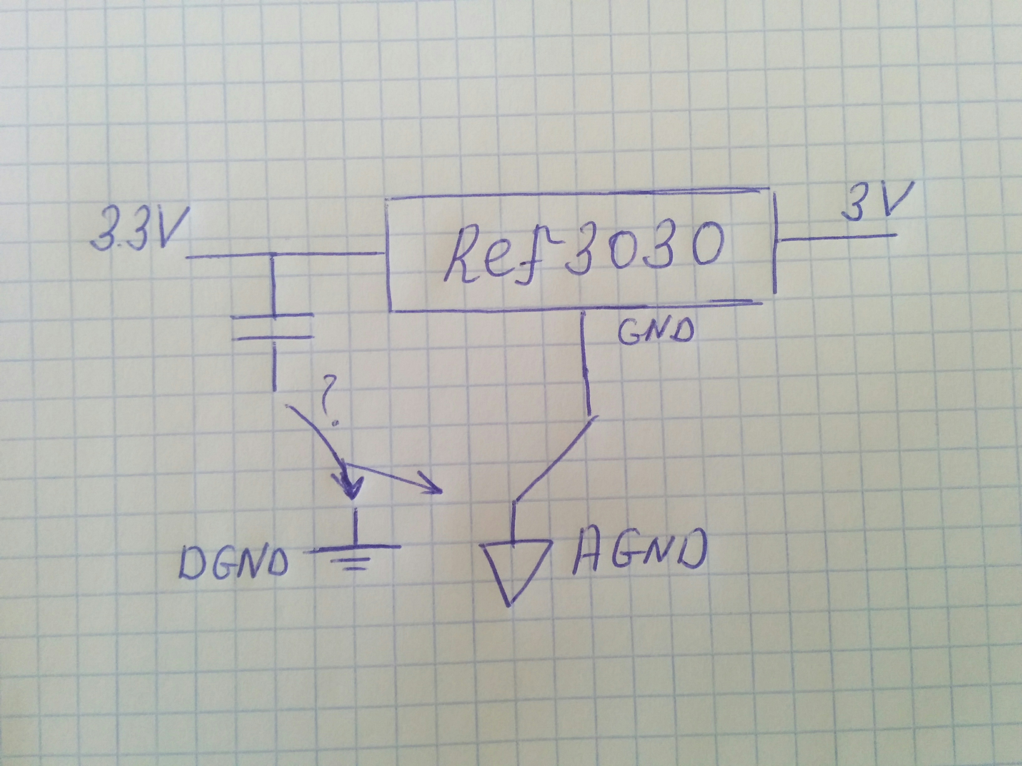
I am designing layout for delfino TMS320F2837xS ,and i am using the REF3030 LDO for ADC VREF,

 i have both DGND and AGND,  my question  is about the REF3030 GND connections :

- should i connect ref3030 ground to the AGND ?

- which ground should i connect to the ref3030 input capacitor?

thank you very much for your help

best regards

Mark

  • Hi Mark,

    My answer would be Analog Ground. For the best results the above 3.3V should be an isolated supply especially for Analog circuitry and should be separated from Digital 3.3V .


    Regards,
    Gautam
  • Hi Mark,

    Use whatever 3.3V rail (and its corresponding ground) that you are using to drive the VDDA pins on the device. You should also use this rail to power the op-amps that buffer the 3.0V signal before driving it to the VREFHI pins - this will help ensure proper power sequencing, as we require VREFHI <= VDDA at all times (there are other ways to accomplish this, but using VDDA to power these buffers is by far the easiest).

    As Gautam said, you want this VDDA rail to be somewhat separate from the VDDIO rail, but also be cautious because we require the delta between VDDIO and VDDA to be no more than 0.3V at any time. One acceptable option to meet this requirement would be to use a single LDO and then separate ferrite beads to separate the rails. Another would be to use identical LDOs to generate the two rails from a common source (you would also want to ensure the VDDA and VDDIO rails have a similar amount of total capacitance, so one rail doesn't ramp significantly faster).

    For the capacitor that goes on the VREFHI pin, put this as close as possible to both the VREFHI and VREFLO pins for that ADC (and then also connect the low side to VSSA nearby).
  • Hi Devin

    thank you very much for the detailed reply , i have attached a schematic part of a board  (i have based my design  on the LAUNCHXL-F28377S) that we have already designed and manufactured ,  but if the current layout needs improvement i will do a second revision.

    i whould be happy if you can give some feedback , from your answer i understand that i needed to power the ref3030 also from VDDA and

    not from the 3.3V  as i did , and then the ref3030 input capacitor  will be referenced to AGND  ? am i right?

    best regards

    Mark

  • Hi Mark,

    This will definitely meet power sequencing requirements because the two OPA320s are powered by VDDA.

    The only concern here is that the REF3030 will not get the benefit of the inductor filter that separates digital 3.3V from VDDA (and in the layout you will have to bring the digital 3.3V / DGND closer to the analog circuitry). If you look at the PSRR characteristics for the REF3030, it is actually a high-pass filter for noise. The inductor is a low-pass filter, so the combo of the two will do a good preventing any noise from coupling from the digital domain into the reference signal.

    I wouldn't worry that this would prevent you from effectively validating your design. If you run into a little bit more noise in the ADC than expected, this would be one possible change to make to try and clean things up.
  • hi Devin

    first of all thank you very much for your great help!

    one last question if i may:

    i am thinking about adding another capacitor after the inductor that will be referenced to digital ground (see option 2) so if any noise will still pass, the returning path will be with the digital ground plane and not move through AGND.

    is there any sense of doing it ?

    best regards

    Mark

  • Hi Mark,


    I think you want option I.  This will prevent noise from bypassing the inductor via the ground plane.