This thread has been locked.

If you have a related question, please click the "Ask a related question" button in the top right corner. The newly created question will be automatically linked to this question.

TMS320F28379D: F2837x controlCARD R1.3 Reference Voltage

Part Number: TMS320F28379D
Other Parts Discussed in Thread: OPA4350, OPA350, REF2030

Hi,

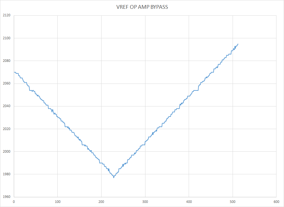
I had a problem in the pas few days with the ADC conversion of the F2837x controlCARD R1.3 and I think we found the source of the problem. Wewere unable to get good conversions with the ADCs. We were always see multiple samples with the same value. By bypassing all the op amp (U13 OPA4350) of the 3.0V voltage reference (U12 REF5030) the conversion results seem to are very good. Could you please confirm that the problem come from the op amp on the devboard. Also could you explain why we get this kind of results with the amplifier on the board. 

Link to my previous posts:

Regards

Dany

  • This appears to be a continuation of this post: e2e.ti.com/.../566150

    Hi Dany,

    This seems better, but still doesn't seem great. The output still appears to have some staircase portions, they are just smaller than before. Can you try the following:

    -Produce a histogram of the converted values instead of a time-series? With this you should be able to see if large chunks of code are systematically missing, or if the staircase portion is randomly occurring. From the plot above, it seems to be the first case - steps with a falling signal are matched by a step in the same place when the signal is rising - but a histogram will be more conclusive.

    -The results you are getting seem to indicate the ADC is not fundamentally working. What is your configured SYSCLK, ADCCLK, and S+H duration? Have you confirmed the SYSCLK by looking at XCLKOUT on a pin? Have you read-back the ADCPRESCALE and other clocking registers to confirm these settings are being written as intended?
  • Hi Devin,

    Thanks for your quick answer. We also noticed that that the staircase portions seem to be at the same location on the signal. We tried different ADCCLK and S+H durations but we didn't notice any difference. We also see that the midscale of the ADC is different if we bypass the op amp. With the original configuration the midscale is arround 2038 and with the op amp bypassed the midscale is arround 2047.

    The configuration for our project is:

    SYSCLK = 200MHz

    ADCCLK = 50MHz

    Sampling window = 100ns

    Conversion time = 220ns

    We will make some tests to look at XCLKOUT on a pin and read-back the ADCPRESCALE and other clocking registers.

    You will find attached an Excel file with the data.

    ADC samples.xlsx

    Best Regards

    Dany

  • Hi Dany,

    I'd definitely recommend measuring the VREF voltage with a DMM in both op-amp and bypass modes. This may be able to account for the change in the middle of your two distributions.

    The other thing you could try would be to bypass the REF3030 but not the OPA350. To do this, remove R60 and populate R59 on the V1.3 ControlCard. You can then source in a VREF voltage through the ADC-VREFHI pin.

    Can you also confirm that SW2 and SW3 are configured for VREFHI from OPA350 and not to select VDDA?
  • Hi Devin,

    We measured the VREF in both modes and the voltage is the same, only the conversion results are different (2038 with opmap, 2047 with bypass opamp).

    We also tried to removed R60 and populate R59 (VREF supplied byREF5030) with the same strange results (staircase).

    Again we tried both configurations (SW2-SW3 all ON and all OFF) and this is how we were able to see that the problem is less significant with VREFHI configured with VDDA. This give us the idea to bypass the OPA4350 to see the results with a reference of 3.0V. This is how we get better results.

    Regards

    Dany
  • Hi Dany,

    What are the settings of the Agilent 33220A?  Is the signal significantly (e.g. factor of 10 or more) gained up or down before being driven into the ADC?

  • Hi Devin,

    Here is the setup for my test:

  • Hi Devin,

    I produced a histogram and as you said we still have some staircase portions even if the opamp are bypassed. Are you able to reproduce the problem with a dev board?

    Dany

  • Hi Dany,

    The reason I asked for the histogram and for the gain was that I was wondering if the resolution of the Agilent 33220A was affecting the results (this instrument has a 14-bit DAC used to generate the signal). If the input signal amplitude is large and then the signal is scaled into the ADC range, or if the input amplitude is really small and it is scaled up then it is possible that you are seeing the resolution of the DAC in the staircases. Why bypassing the reference helps also makes sense; you are effectively adding noise to the input, which helps spread it out and hide the resolution issues.

    Looking at your diagram though, the resolution shouldn't be a problem; you start with a reasonable signal amplitude of 1V and then scale it down, which should improve the effective resolution (is the input signal 0VDC + 1Vpp, if it had a huge DC offset maybe it would be a problem?).

    You can at least rule this out by supplying a 63.5mVpp signal directly to the ADC and seeing if that looks ok or if it still has the missing codes.

    I'm not sure if I'll get a chance to try this with a ControlCard in the next few days, but our internal characterization boards have the same OPA350 VREFHI driver circuit and work great.
  • Hi Devin,

    Thanks again for your help.

    As you mentioned the Agilent input signal is 0VDC + 1Vpp. At the ADC the signal is 63.5mVpp with an offset of 1.5V generated by the REF2030. We already tried to supply a 63.5Vpp signal directly to the ADC with the same result (the voltage reference was buffered with the OPA350).

    Do you think there is a way to improve the signal conversion? I'm still not sure why the OPA350 has this effect to the converted signal?

    Dany
  • Hi Dany,

    Sorry about the delay. I was able to replicate the issue on R1.3 ControlCard. This can be resolved by replacing R51-R54 with a 0.1ohm resistor (this is what is called for in the BOM and schematic, but it appears they were manufactured with 100M instead). It is also likely that the performance will be good with a 0-ohm resistor or just a solder bridge between the resistor pads.