This thread has been locked.

If you have a related question, please click the "Ask a related question" button in the top right corner. The newly created question will be automatically linked to this question.

CCS/TMS320F28027F: How much is the minimum Power Consumption of TMS320F28027F

Part Number: TMS320F28027F

Tool/software: Code Composer Studio

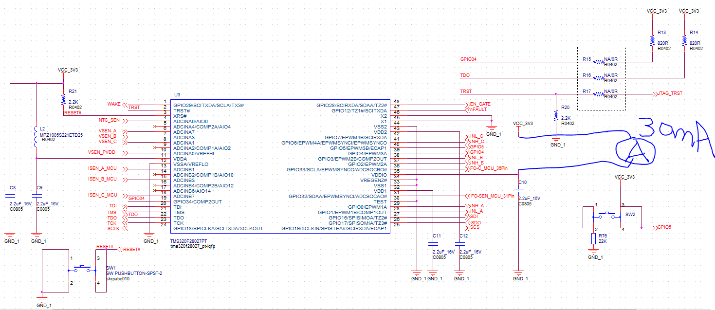
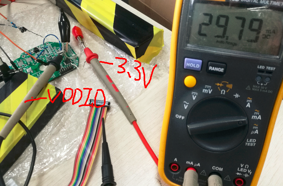
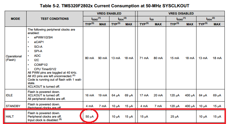
How much is the minimum Power Consumption  of  TMS320F28027F ?   Download  Example_F2802xHaltWake into the TMS320F28027F;   the current measured is 5mA.

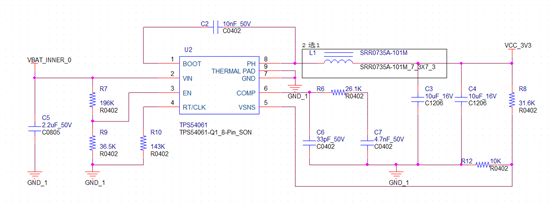
电源系统用的是TPS54061,该电源在24V供电下静态功耗在测得有256uA。(没有接任何负载)

The power supply system with   TPS54061,Power in 24 V power supply,  Current Consumption have 256uA.(there is No load)

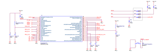
The entire board welding with a minimum system, and a download the circuit. Runninng Example_F2802xHaltWake ,the Current Consumption is 5mA,and then wake up the Current Consumption is 10mA.

How much is the minimum Power Consumption of  TMS320F28027F? Could I reduce it more?

  • Hello,

    The device level power consumption information is in the device datasheet. www.ti.com/.../tms320f28027.pdf . See sections 5.4 Power Consumption Summary and 6.1.15 Low-power Modes for more information.

    Halt mode is the lowest power state of the device, essentially one step above being powered down, so there is not much more that you can do. Please verify that the Flash bank is powered down, and that you have disabled the internal Oscillator during halt mode (CLKCTL.INTOSC1HALTI and CLKCTL.INTOSC2HALTI are both 0 -the default). Note that if the internal oscillators are turned off during halt mode, the wake up time will increase.

    What board are you using? is it a custom board? If so, how are you measuring the power consumption of the device? Are there any additional components on the regulator output?
  • The source code: I refer to the  Example_F2802xHaltWake  and remove   wakeint_isr

    void main(void)
    {
    CPU_Handle myCpu;
    PLL_Handle myPll;
    PWR_Handle myPwr;
    WDOG_Handle myWDog;

    // Initialize all the handles needed for this application
    myClk = CLK_init((void *)CLK_BASE_ADDR, sizeof(CLK_Obj));
    myCpu = CPU_init((void *)NULL, sizeof(CPU_Obj));
    myFlash = FLASH_init((void *)FLASH_BASE_ADDR, sizeof(FLASH_Obj));
    myGpio = GPIO_init((void *)GPIO_BASE_ADDR, sizeof(GPIO_Obj));
    myPie = PIE_init((void *)PIE_BASE_ADDR, sizeof(PIE_Obj));
    myPll = PLL_init((void *)PLL_BASE_ADDR, sizeof(PLL_Obj));
    myPwr = PWR_init((void *)PWR_BASE_ADDR, sizeof(PWR_Obj));
    myWDog = WDOG_init((void *)WDOG_BASE_ADDR, sizeof(WDOG_Obj));

    //Select the internal oscillator 1 as the clock source
    CLK_setOscSrc(myClk, CLK_OscSrc_Internal);

    // Setup the PLL for x10 /2 which will yield 50Mhz = 10Mhz * 10 / 2
    PLL_setup(myPll, PLL_Multiplier_12, PLL_DivideSelect_ClkIn_by_2);

    // Disable the PIE and all interrupts
    PIE_disable(myPie);
    PIE_disableAllInts(myPie);
    CPU_disableGlobalInts(myCpu);
    CPU_clearIntFlags(myCpu);

    // If running from flash copy RAM only functions to RAM
    #ifdef _FLASH
    memcpy(&RamfuncsRunStart, &RamfuncsLoadStart, (size_t)&RamfuncsLoadSize);
    #endif

    // Initalize GPIO
    // Enable Pull-ups
    GPIO_setPullUp(myGpio, GPIO_Number_5, GPIO_PullUp_Enable);

    // Choose GPIO0 pin for lpm wakeup
    GPIO_lpmSelect(myGpio,GPIO_Number_5);

    // Only enter Standby mode when PLL is not in limp mode.
    if ( PLL_getClkStatus(myPll) != PLL_PLLSTS_MCLKSTS_BITS)
    {
    // LPM mode = Standby
    PWR_setLowPowerMode(myPwr, PWR_LowPowerMode_Halt);
    }

    CLK_disableAdcClock(myClk);

    // Force device into STANDBY
    IDLE; // Device waits in IDLE until falling edge on GPIO0/XNMI pin
    // wakes device from Standby mode.
    for(;;){} // Loop here after wake-up.

    }


       What should I do ?

  • There are nothing another loads;only power supply and TMS320F28027F microcontroller minimum system.

  • Hmm,

    The code looks unmodified, and it appears that it is setting the device into halt mode. By default it looks like the flash is still probably powered on. Please go through the F28027 System Control and Interrupts User Guide Section Section 1.3 Flash
    and OTP Power Modes for more information. www.ti.com/.../sprufn3d.pdf

    Can you share exactly where and how you are measuring the power consumption of the device. Are you mesuring a voltage drop across a shunt resistor, putting an ammeter between the output of the TPS and the MCU? I cannot zoom into your schematic image. Please increase the size, or use the attach feature so the image can be clicked.
  • void main()
    {
    // WARNING: Always ensure you call memcpy before running any functions from RAM
    // InitSysCtrl includes a call to a RAM based function and without a call to
    // memcpy first, the processor will go "into the weeds"

    memcpy(&RamfuncsRunStart, &RamfuncsLoadStart, (size_t)&RamfuncsLoadSize);

    // Step 1. Initialize System Control:
    // PLL, WatchDog, enable Peripheral Clocks


    EALLOW;
    SysCtrlRegs.CLKCTL.bit.INTOSC1OFF = 0;
    SysCtrlRegs.CLKCTL.bit.OSCCLKSRCSEL=0; // Clk Src = INTOSC1
    SysCtrlRegs.CLKCTL.bit.XCLKINOFF=1; // Turn off XCLKIN
    SysCtrlRegs.CLKCTL.bit.XTALOSCOFF=1; // Turn off XTALOSC
    SysCtrlRegs.CLKCTL.bit.INTOSC2OFF=1; // Turn off INTOSC2


    EDIS;

    InitPll(6,3);

    // Step 2. Initalize GPIO:
    // Enable all pull-ups
    EALLOW;
    GpioCtrlRegs.GPAPUD.bit.GPIO4 = 0;
    GpioIntRegs.GPIOLPMSEL.bit.GPIO4 = 1; // Choose GPIO4 pin for wakeup

    // Make GPIO6 an input
    GpioCtrlRegs.GPAMUX1.bit.GPIO5 = 0; // GPIO5 = GPIO5
     GpioCtrlRegs.GPADIR.bit.GPIO5 = 0; // GPIO5 = input


    SysCtrlRegs.PCLKCR0.bit.ADCENCLK = 0; // ADC

    SysCtrlRegs.PCLKCR3.bit.COMP1ENCLK = 0; // COMP1
    SysCtrlRegs.PCLKCR3.bit.COMP2ENCLK = 0; // COMP2
    SysCtrlRegs.PCLKCR3.bit.CPUTIMER0ENCLK = 0; // CPU Timer-0
    SysCtrlRegs.PCLKCR3.bit.CPUTIMER1ENCLK = 0; // CPU Timer-1
    SysCtrlRegs.PCLKCR3.bit.CPUTIMER2ENCLK = 0; // CPU Timer-2
    SysCtrlRegs.PCLKCR3.bit.rsvd4 = 0; // COMP1

    SysCtrlRegs.PCLKCR1.bit.ECAP1ENCLK = 0; // eCAP1
    SysCtrlRegs.PCLKCR1.bit.EPWM1ENCLK = 0; // EPWM1
    SysCtrlRegs.PCLKCR1.bit.EPWM2ENCLK = 0; // EPWM2
    SysCtrlRegs.PCLKCR1.bit.EPWM3ENCLK = 0; // EPWM3
    SysCtrlRegs.PCLKCR1.bit.EPWM4ENCLK = 0; // EPWM4

    SysCtrlRegs.PCLKCR3.bit.GPIOINENCLK = 0; // GPIO

    SysCtrlRegs.PCLKCR0.bit.HRPWMENCLK= 0; // HRPWM
    SysCtrlRegs.PCLKCR0.bit.I2CAENCLK = 0; // I2C
    SysCtrlRegs.PCLKCR0.bit.SCIAENCLK = 0; // SCI-A
    SysCtrlRegs.PCLKCR0.bit.SPIAENCLK = 0; // SPI-A
    SysCtrlRegs.PCLKCR0.bit.TBCLKSYNC = 0; // Enable TBCLK within the EPWM

    EDIS;

    // Initialize the PIE control registers to their default state.
    // The default state is all PIE interrupts disabled and flags
    // are cleared.
    // This function is found in the f2802x_PieCtrl.c file.
    InitPieCtrl();

    // Disable CPU interrupts and clear all CPU interrupt flags:
    IER = 0x0000;
    IFR = 0x0000;

    // Initialize the PIE vector table with pointers to the shell Interrupt
    // Service Routines (ISR).
    // This will populate the entire table, even if the interrupt
    // is not used in this example. This is useful for debug purposes.
    // The shell ISR routines are found in f2802x_DefaultIsr.c.
    // This function is found in f2802x_PieVect.c.
    InitPieVectTable();

    // Interrupts that are used in this example are re-mapped to
    // ISR functions found within this file.
    EALLOW; // This is needed to write to EALLOW protected registers
    PieVectTable.WAKEINT = &WAKE_ISR;
    EDIS;

    // Step 4. Initialize all the Device Peripherals:
    // Not applicable for this example.

    // Step 5. User specific code, enable interrupts:

    // Enable CPU INT1 which is connected to WakeInt:
    IER |= M_INT1;

    // Enable WAKEINT in the PIE: Group 1 interrupt 8
    PieCtrlRegs.PIEIER1.bit.INTx8 = 1;
    PieCtrlRegs.PIEACK.bit.ACK1 = 1;
    // Enable global Interrupts:
    EINT; // Enable Global interrupt INTM

    // Write the LPM code value
    EALLOW;
    if (SysCtrlRegs.PLLSTS.bit.MCLKSTS != 1) // Only enter low power mode when PLL is not in limp mode.
    {
    //SysCtrlRegs.LPMCR0.bit.LPM = 0x0001; // LPM mode = STANDBY

    SysCtrlRegs.LPMCR0.bit.LPM = 0x0002; // LPM mode = Halt

    }
    EDIS;

    // wakes device from halt mode.
    for(;;)
    {

    if( GpioDataRegs.GPADAT.bit.GPIO5 == 1 )
    {
    EALLOW; // This is needed to write to EALLOW protected registers

    __asm(" IDLE");

    EDIS;
    }
    }// Loop here after wake-up.

    }

    /* ----------------------------------------------- */
    /* ISR for WAKEINT - Will be executed when */
    /* low pulse triggered on GPIO0 pin */
    /* ------------------------------------------------*/
    __interrupt void WAKE_ISR(void)
    {
      LPWR_count++;

      PieCtrlRegs.PIEACK.bit.ACK1 = 1;
    }

    Set   LPM mode == STANDBY

    SysCtrlRegs.LPMCR0.bit.LPM = 0x0001; // LPM mode = STANDBY

    or   LPM mode == HALT

    SysCtrlRegs.LPMCR0.bit.LPM = 0x0002; // LPM mode = HALT

    both of he IDDIO  value is 30mA !!!!!

    but in datasheet  the  IDDIO value is only 4-7mA.  How did you test?  could you give me some advises.

    There are nothing another loads;only power supply and TMS320F28027F microcontrol  minimum system.

  • Hi there, sorry about the late reply. I duplicated your test on my bench set up. You have not powered down the flash. Please add the following lines of code. Ensure that the code that powers down the flash is executed from RAM and that any subsequent instructions are also run from RAM, otherwise the Flash will be powered on before the devices enters the LPM.

    EALLOW;
    FlashRegs.FPWR.bit.PWR = 0;
    EDIS;

    Thanks,
    Mark