This thread has been locked.

If you have a related question, please click the "Ask a related question" button in the top right corner. The newly created question will be automatically linked to this question.

TMS320F2812: some I/O pins were unstable

Part Number: TMS320F2812


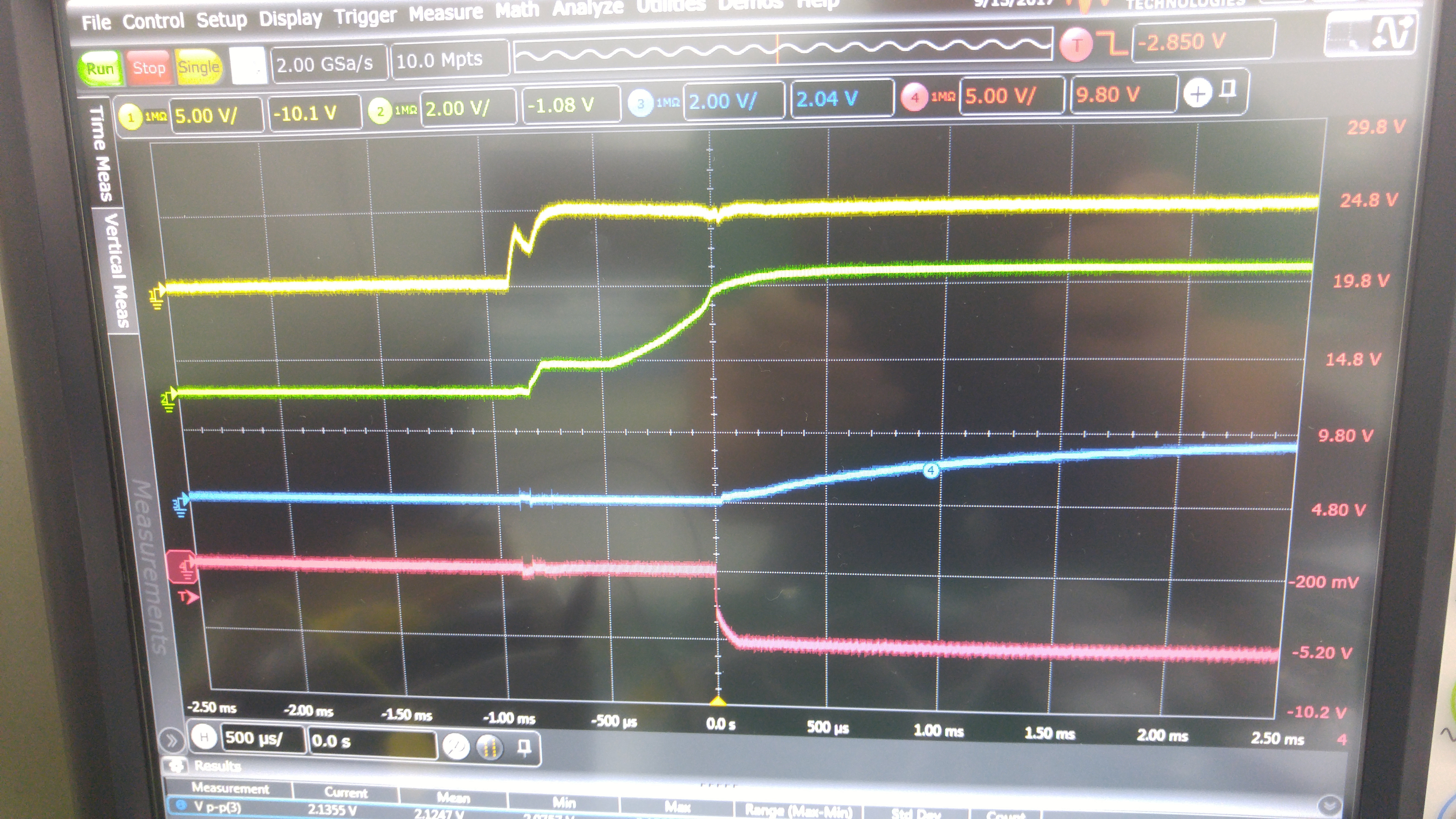
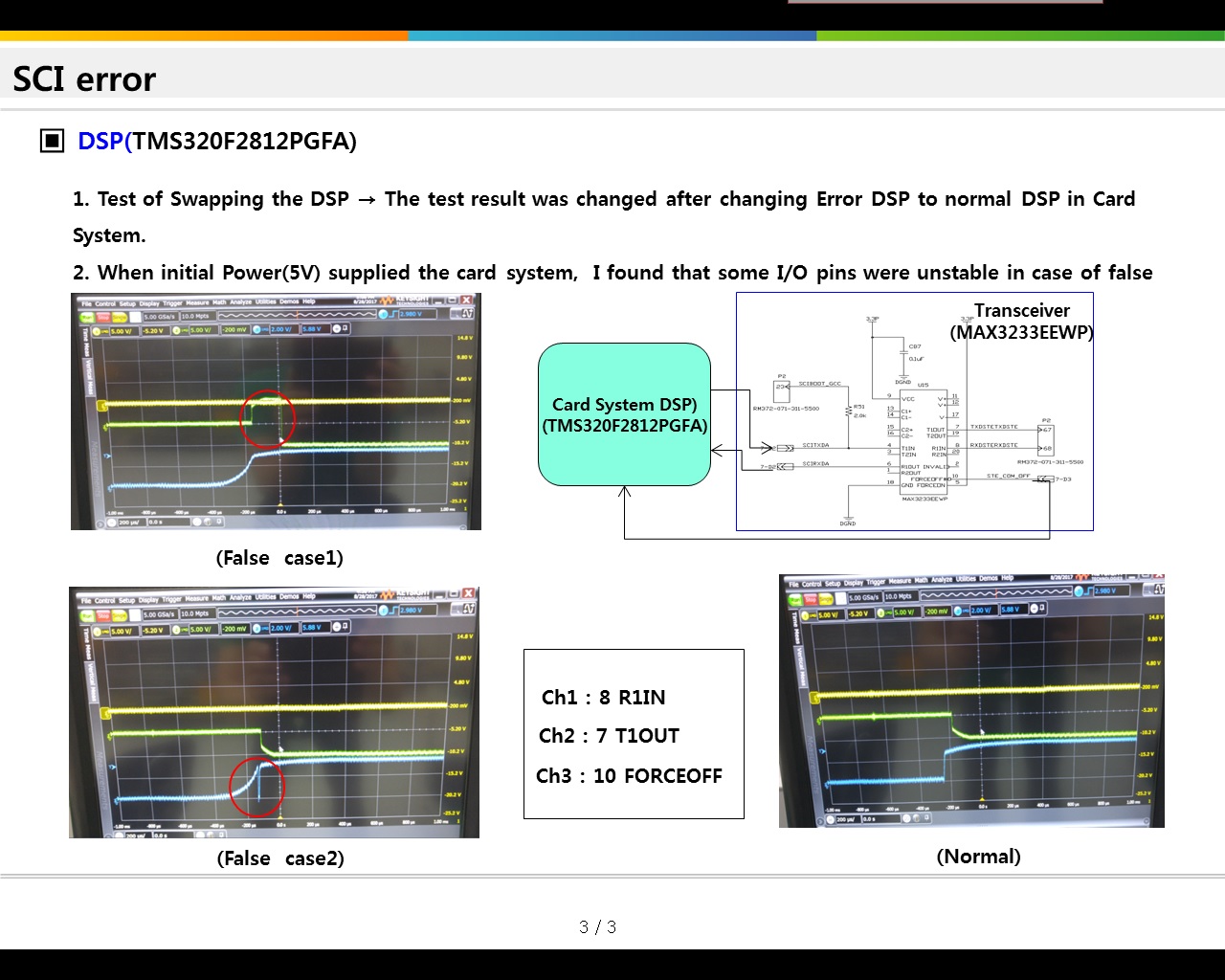
I found that some I/O pins were unstable when power supplied the our system(circuit card).  Because of this issue, we have a communication problem using the SCI in the DSP. Most of DSPs which we have are stable but a few DSPs are unstable.  Unstable DSPs were supplied by initial power,  SCITXD line generated an unexpected pulse(duty of 200 us).  we even took a test swapping the DSPs -> The test result was exchanged after changing unstable DSPs to stable DSPs in our system.
Please let me know unstable DSPs are normal status or false status.
Regards,

  • Hi Green,

    Please note the F281x power sequencing requirements.  These can be found within the "Power Sequencing Requirements" section of the datasheet.  Please also be aware of the NOTE in that section.  It states that the state of GPIO pins will be undefined until VDD = 1V and VDDIO = 2.5V.

    Therefore, what you are seeing should be expected.  I would recommend editing the C2000 software to make it immune to glitching.  One option for doing this might be to add software delays before using the SCI communication link.

    C2000 has made improvements in newer devices so that power sequencing is simpler, and so that glitching does not occur.

    Hopefully the helps!


    Thank you,
    Brett

  • Dear Brett,

    Thank you for your advice.

    I've got that problem. A few DSPs(TMS320F2812) which I have often(40% probability) generate unexpected pulses when the initial power is applied, regardless of the system( circuit cards). but most of DSPs(TMS320F2812) which I have do not(never produce an unexpeced pulse).

    My system(circuit card) already has a LDO regulator(P/N : TPS767D301PWP) for the power sequencing requirements .
    Could you tell me if the DSPs with unstable I/Os are defective or not?

    Regards,
    Nohyun
  • Hi Nohyun,

    They are not defective.  As mentioned, GPIOs on this device will be in an undefined state as the device powers up (and it is also possible for the state to change during this time).  Some devices may produce glitches more often, but conditions (temperature, voltages, etc) may also affect the probability.

    You will need to add software in your SCI/UART network/drivers so that it is robust against potential glitching during the power up of C2000 devices.


    Thank you,
    Brett

  • Dear Brett,

    Thank you for your help.

    .

    I have another picture with glitches regarding the DSP(TMS320F2812). as you can see the glitch occured in this  pitcture after power is stable( 200 us).

    The ch2:green line is SCITXA and ch3:blue line is Forceoff conneted with DSP I/O pin.

    The test condition is  25 ºC(room temperature) and 5 V (applied voltage)

    I think that this situation is a little bit different with your explanaiton.(it is not an undefined state.)

    Is this DSP also normal? I need your advice.

    Regards,

    Nohyun

  • Hi Nohyun,

    It appears that you're measuring your signal between the transceivers.  What does the waveform look like between the C2000 device and the transceiver? 

    It would also be helpful for me to see the power rails in the screenshot you take.

    ===

    Does "5V applied voltage" mean that the transceiver is powered with 5V?


    Thank you,
    Brett

  • Dear Brett,

    The screen shot of SCI error page and above screen shot are measuring the same position of the transceiver.(Ch1 :8, Ch2:7, Ch3:8)
    The DSP is powered with 3.3 V and 1.9V and the transceiver is powered with 3.3 V through the LDO regulator with 5V input.
    Unfortunately, there is no power rails in the screenshots I have.
    The DSPs which has glitch in our circuit are already fixed as changing the DSPs.

    Thank you,
    Nohyun
  • Hi Nohyun,

    The data provided isn't enough for me to say whether the root cause is with the chip or with the system design.  Screenshots such as the one I've requested would bring us the information needed to debug further.

    In Green Deng's post, it is stated that 'most' devices are stable, but 'a few' are unstable.  What is the ratio?


    Thank you,
    Brett

  • Hi Brett,

    I got screenshots which you request. In the pictures → ch1(yellow) : 5V, ch2(green) : 3.3V, ch3(blue) : 1.9V, ch4(red) : SCITX

    please, review the attachments.

    and the ratio of unstable DSPs is around 10%.

    Regards,

    Nohyun

  • Hi Nohyun,

    Thank you for these images. 

    The glitching on the red signal appears to be occurring before VDD (1.9V) becomes greater than 1V. 

    According to the datasheet, the output of GPIO pins will be undefined until VDD (1.8V or 1.9V) > 1V    and   VDDIO (3.3V) > 2.5V.


    Thank you,
    Brett