This thread has been locked.

If you have a related question, please click the "Ask a related question" button in the top right corner. The newly created question will be automatically linked to this question.

TMS320F28035: LIN Registers Not Updating

Part Number: TMS320F28035
Other Parts Discussed in Thread: CONTROLSUITE, C2000WARE

Hi

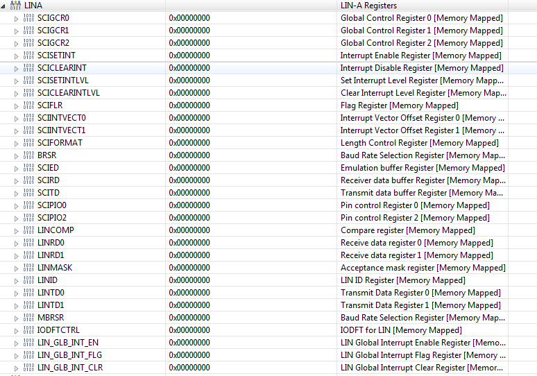
I am doing the LIN configuration in its registers but LIN registers are not getting updated in the "Registers" View.

Tried Control Suite  LIN related example and there also couldn't see registers getting updated. 

Please find the attached LIN configuration code and images of the "Registers" View and help me solve this issue.

void LIN_Init(void)
{	
    EALLOW; // This is needed to write to EALLOW protected registers
    PieVectTable.LIN0INTA = &Lin_Level0_ISR;
    PieVectTable.LIN1INTA = &Lin_Level1_ISR;
   	EDIS;   // This is needed to disable write to EALLOW protected registers

	/* Enable LINA_INT1 to LINA_INT0 in PIE */
    PieCtrlRegs.PIECTRL.bit.ENPIE = 1;    // Enable the PIE block
    PieCtrlRegs.PIEIER9.bit.INTx3 = 1;    // PIE Group 9, INT3
    PieCtrlRegs.PIEIER9.bit.INTx4 = 1;    // PIE Group 9, INT4
    IER = 0x100;	// Enable CPU INT
    EINT;

	EALLOW;

	/* Module Reset*/
	LinaRegs.SCIGCR0.bit.RESET 			= 0; 
	 
	/* Pull module out of reset */
    LinaRegs.SCIGCR0.bit.RESET 			= 1;  
	   
	/* The BLIN is in its reset state; no data will be transmitted 
	or received. */
    LinaRegs.SCIGCR1.bit.SWnRST 		= 0;

	LinaRegs.SCIGCR1.bit.LINMODE 		= 1;	
	
	/* LIN node is in  mode  */
    LinaRegs.SCIGCR1.bit.CLK_MASTER 	= 1;//LIN_SLAVEMODE

	/* LIN Automatic baudrate adjustment is enabled according to LIN Master */

    LinaRegs.SCIGCR1.bit.ADAPT          = 0;

    LinaRegs.BRSR.bit.SCI_LIN_PSL = 96;                 // 19.2 kbps
    LinaRegs.BRSR.bit.M = 11;
    LinaRegs.MBRSR = 92; //20kHz (max autobaud rate)


	/* In LIN mode ID4 and ID5 are not used for 
	length control */ 
    LinaRegs.SCIGCR1.bit.COMMMODE 		= 0;   
	
	/* Continue on Suspend, the SCI/BLIN continues to operate until the current
    transmit and receive functions are complete */
    LinaRegs.SCIGCR1.bit.CONT 			= 1;	
	
	LinaRegs.SCIGCR1.bit.CTYPE 			= 1;
	
	/* ID filtering using ID-SlaveTask byte, RECID and ID-Slave task byte are 
	used for detecting a match */
	LinaRegs.SCIGCR1.bit.HGENCTRL 		= 1;
	
	/* Loop back mode is disabled */
    LinaRegs.SCIGCR1.bit.LOOPBACK 		= 0; 
	
	/* RX/TX multibuffers are used */
    LinaRegs.SCIGCR1.bit.MBUFMODE 		= 1;	
	
	/*         Parity Check */
    LinaRegs.SCIGCR1.bit.PARITYENA 		= 1;
	
	/* Enable TX, Enable transfers of data from SCITD or TDy to SCITXSHF */
    LinaRegs.SCIGCR1.bit.RXENA 			= 1;
	
	/* Enable RX, Allows the receiver to transfer data from the shift buffer to 
	the receive buffer or multi-buffers */
    LinaRegs.SCIGCR1.bit.TXENA 			= 1;
	
	/* Validate checksum */
	LinaRegs.SCIGCR2.bit.CC 			= 1; 	

	/* Set all interrupts to disabled */
    LinaRegs.SCICLEARINT.all 		    = 0xFFFFFFFF;	
	
	LinaRegs.SCIFORMAT.bit.LENGTH 	= 0;
	 
	/* SYNC Field Configuration */
	/* Sync break is 13 + 5 = 18 Tbits */
    LinaRegs.LINCOMP.bit.SBREAK 		= 5; 
	/* Sync delimiter is 1 + 3 = 4 Tbits */
    LinaRegs.LINCOMP.bit.SDEL 			= 3; 	

    /* LIN MASK, allow all ID reception */
    LinaRegs.LINMASK.bit.RXIDMASK 		= 0xFF;  
    LinaRegs.LINMASK.bit.TXIDMASK 		= 0xFF;	
	
    /* Ensure IODFT (used to force different error conditions) is disabled */
    LinaRegs.IODFTCTRL.bit.IODFTENA 	= 0;
	LinaRegs.IODFTCTRL.bit.LPBENA 	 	= 0;
	 
	/* Pull out of software reset */
    LinaRegs.SCIGCR1.bit.SWnRST 		= 1;  	 

	EDIS;
	
	EALLOW;
	
	/* Under Reset */
    LinaRegs.SCIGCR1.bit.SWnRST 		= 0; 
	
	LinaRegs.SCIGCR1.bit.PARITYENA 		= 0;
	
//	LinaRegs.SCISETINT.all 				= 0xFFFFFFFF;
	
     LinaRegs.SCISETINT.bit.SETIDINT     = 1;//IDINT
     LinaRegs.SCISETINT.bit.SETRXINT     = 1;//RXINT
     LinaRegs.SCISETINT.bit.SETTXINT     = 1;//TXINT
     LinaRegs.SCISETINT.bit.SETWAKEUPINT = 1;

	LinaRegs.SCICLEARINTLVL.all         = 0xFFFFFFFF;		// Interrupt asserted in INT0
	
	LinaRegs.LINMASK.bit.RXIDMASK = 0xA;  
    LinaRegs.LINMASK.bit.TXIDMASK = 0xA;  
	
	/* Initialize the Slave LINIDNUM register */
	LinaRegs.LINID.bit.IDSLAVETASKBYTE  = 0x30;      
	
	/* Pull out of software reset */
    LinaRegs.SCIGCR1.bit.SWnRST 		= 1;  
	
	/* Number of bytes in the response field */
    LinaRegs.SCIFORMAT.bit.LENGTH 		= 7;
		
	/* Intialize LIN state to LIN_INIT */
    LIN_Status  = LIN_INIT;
	
    /* Intialize the LIN ID */
    LIN_Id 	    = ZERO;
	
    /* Intialize the recieve wait time count */
    LIN_RecWaitTime = ZERO;

    /* Intialize the communication time count */
    LIN_CommTime 	= ZERO;

    /* Intialize the LIN recive wait timeout status */
    LIN_RecWaitErrSt = FALSE;

    if(LIN_RecWaitErrSt);
	
	EDIS;

}

Regards

Mayank Bhatt

  • Mayank,

    All zeros in the registers is usually an indication that the clock to the peripheral has not been enabled
    When you run the example, make sure to go past the point where the clocks are enabled before viewing the registers.

    void InitPeripheralClocks(void) is the function where this occurs.

    If this does not work, please indicate the version of the example and what you have tried to debug the issue.

    Regards
    Lori
  • Lori

    Thanks for the swift reply.

    I already checked Clock to LIN peripheral which is enabled in the example code, I'm referring control suit example code (lina_external_loopback) and doing similar LIN registers configuration in my code with little changes as per my requirement .

    Code skeleton is attached.

    void LIN_Init(void)
    {	
        EALLOW; // This is needed to write to EALLOW protected registers
        PieVectTable.LIN0INTA = &Lin_Level0_ISR;
        PieVectTable.LIN1INTA = &Lin_Level1_ISR;
       	EDIS;   // This is needed to disable write to EALLOW protected registers
    
    	/* Enable LINA_INT1 to LINA_INT0 in PIE */
        PieCtrlRegs.PIECTRL.bit.ENPIE = 1;    // Enable the PIE block
        PieCtrlRegs.PIEIER9.bit.INTx3 = 1;    // PIE Group 9, INT3
        PieCtrlRegs.PIEIER9.bit.INTx4 = 1;    // PIE Group 9, INT4
        IER = 0x100;	// Enable CPU INT
        EINT;
    
    	EALLOW;
    
    	/* Module Reset*/
    	LinaRegs.SCIGCR0.bit.RESET 			= 0; 
    	 
    	/* Pull module out of reset */
        LinaRegs.SCIGCR0.bit.RESET 			= 1;  
    	   
    	/* The BLIN is in its reset state; no data will be transmitted 
    	or received. */
        LinaRegs.SCIGCR1.bit.SWnRST 		= 0;
    
    	LinaRegs.SCIGCR1.bit.LINMODE 		= 1;	
    	
    	/* LIN node is in  mode  */
        LinaRegs.SCIGCR1.bit.CLK_MASTER 	= 1;//LIN_SLAVEMODE
    
    	/* LIN Automatic baudrate adjustment is enabled according to LIN Master */
    
        LinaRegs.SCIGCR1.bit.ADAPT          = 0;
    
        LinaRegs.BRSR.bit.SCI_LIN_PSL = 96;                 // 19.2 kbps
        LinaRegs.BRSR.bit.M = 11;
        LinaRegs.MBRSR = 92; //20kHz (max autobaud rate)
    
    
    	/* In LIN mode ID4 and ID5 are not used for 
    	length control */ 
        LinaRegs.SCIGCR1.bit.COMMMODE 		= 0;   
    	
    	/* Continue on Suspend, the SCI/BLIN continues to operate until the current
        transmit and receive functions are complete */
        LinaRegs.SCIGCR1.bit.CONT 			= 1;	
    	
    	LinaRegs.SCIGCR1.bit.CTYPE 			= 1;
    	
    	/* ID filtering using ID-SlaveTask byte, RECID and ID-Slave task byte are 
    	used for detecting a match */
    	LinaRegs.SCIGCR1.bit.HGENCTRL 		= 1;
    	
    	/* Loop back mode is disabled */
        LinaRegs.SCIGCR1.bit.LOOPBACK 		= 0; 
    	
    	/* RX/TX multibuffers are used */
        LinaRegs.SCIGCR1.bit.MBUFMODE 		= 1;	
    	
    	/*         Parity Check */
        LinaRegs.SCIGCR1.bit.PARITYENA 		= 1;
    	
    	/* Enable TX, Enable transfers of data from SCITD or TDy to SCITXSHF */
        LinaRegs.SCIGCR1.bit.RXENA 			= 1;
    	
    	/* Enable RX, Allows the receiver to transfer data from the shift buffer to 
    	the receive buffer or multi-buffers */
        LinaRegs.SCIGCR1.bit.TXENA 			= 1;
    	
    	/* Validate checksum */
    	LinaRegs.SCIGCR2.bit.CC 			= 1; 	
    
    	/* Set all interrupts to disabled */
        LinaRegs.SCICLEARINT.all 		    = 0xFFFFFFFF;	
    	
    	LinaRegs.SCIFORMAT.bit.LENGTH 	= 0;
    	 
    	/* SYNC Field Configuration */
    	/* Sync break is 13 + 5 = 18 Tbits */
        LinaRegs.LINCOMP.bit.SBREAK 		= 5; 
    	/* Sync delimiter is 1 + 3 = 4 Tbits */
        LinaRegs.LINCOMP.bit.SDEL 			= 3; 	
    
        /* LIN MASK, allow all ID reception */
        LinaRegs.LINMASK.bit.RXIDMASK 		= 0xFF;  
        LinaRegs.LINMASK.bit.TXIDMASK 		= 0xFF;	
    	
        /* Ensure IODFT (used to force different error conditions) is disabled */
        LinaRegs.IODFTCTRL.bit.IODFTENA 	= 0;
    	LinaRegs.IODFTCTRL.bit.LPBENA 	 	= 0;
    	 
    	/* Pull out of software reset */
        LinaRegs.SCIGCR1.bit.SWnRST 		= 1;  	 
    
    	EDIS;
    	
    	EALLOW;
    	
    	/* Under Reset */
        LinaRegs.SCIGCR1.bit.SWnRST 		= 0; 
    	
    	LinaRegs.SCIGCR1.bit.PARITYENA 		= 0;
    	
    //	LinaRegs.SCISETINT.all 				= 0xFFFFFFFF;
    	
         LinaRegs.SCISETINT.bit.SETIDINT     = 1;//IDINT
         LinaRegs.SCISETINT.bit.SETRXINT     = 1;//RXINT
         LinaRegs.SCISETINT.bit.SETTXINT     = 1;//TXINT
         LinaRegs.SCISETINT.bit.SETWAKEUPINT = 1;
    
    	LinaRegs.SCICLEARINTLVL.all         = 0xFFFFFFFF;		// Interrupt asserted in INT0
    	
    	LinaRegs.LINMASK.bit.RXIDMASK = 0xA;  
        LinaRegs.LINMASK.bit.TXIDMASK = 0xA;  
    	
    	/* Initialize the Slave LINIDNUM register */
    	LinaRegs.LINID.bit.IDSLAVETASKBYTE  = 0x30;      
    	
    	/* Pull out of software reset */
        LinaRegs.SCIGCR1.bit.SWnRST 		= 1;  
    	
    	/* Number of bytes in the response field */
        LinaRegs.SCIFORMAT.bit.LENGTH 		= 7;
    		
    	/* Intialize LIN state to LIN_INIT */
        LIN_Status  = LIN_INIT;
    	
        /* Intialize the LIN ID */
        LIN_Id 	    = ZERO;
    	
        /* Intialize the recieve wait time count */
        LIN_RecWaitTime = ZERO;
    
        /* Intialize the communication time count */
        LIN_CommTime 	= ZERO;
    
        /* Intialize the LIN recive wait timeout status */
        LIN_RecWaitErrSt = FALSE;
    
        if(LIN_RecWaitErrSt);
    	
    	EDIS;
    }
    
    
    void LINTxData(void)
    {
        /* Put 4 bytes in LIN Transmit Buffer 0 Register */
        LinaRegs.LINTD0.bit.TD0 = 0x55; 
        LinaRegs.LINTD0.bit.TD1 =  0x55;
        LinaRegs.LINTD0.bit.TD2 =  0x55;
        LinaRegs.LINTD0.bit.TD3 =  0x55;
    
        /* Put 4 bytes in LIN Transmit Buffer 1 Register */
        LinaRegs.LINTD1.bit.TD4 =  0x55;
        LinaRegs.LINTD1.bit.TD5 =  0x55;
        LinaRegs.LINTD1.bit.TD6 =  0x55;
        LinaRegs.LINTD1.bit.TD7 =  0x55;
    
        LinaRegs.LINID.bit.IDBYTE =  0x1F;
    }


    void main(void)
    {
       MCU_Init();
       EALLOW;
       SysCtrlRegs.PCLKCR0.bit.LINAENCLK    = (uint8)1;
    	
       GpioCtrlRegs.GPAPUD.bit.GPIO22 		= (uint8)0;		// Enable pull-up for GPIO22 (LIN TX)
    	
       GpioCtrlRegs.GPAPUD.bit.GPIO23 		= (uint8)0;		// Enable pull-up for GPIO23 (LIN RX)
    	
       GpioCtrlRegs.GPAQSEL2.bit.GPIO23 	= (uint8)3;  // Asynch input GPIO23 (LINRXA)
    	
       /* Set GPIO23 as LIN_RXD */
       GpioCtrlRegs.GPAMUX2.bit.GPIO23      = (uint8)3;
    
       /* Set GPIO22 as LIN_TXD */
       GpioCtrlRegs.GPAMUX2.bit.GPIO22      = (uint8)3;
       EDIS;
    
    // Step 3. Clear all interrupts and initialize PIE vector table:
    // Disable CPU interrupts
       DINT;
       
       InitPieCtrl();
    
       	//Disable CPU interrupts and clear all CPU interrupt flags:
        IER = 0x0000;
        IFR = 0x0000;
    	
       InitPieVectTable();
      
       LIN_Init();
       TIMER_Init();
       RTSC_Scheduler();  // LIN data transmission (LINTxData())is called from here 
    
       while(1)
       {
    
       }
       
    }


    __interrupt void Lin_Level0_ISR(void)
    {
    	/* Using for local logical operations */
        uint32 error_data;
        UnpackRxBuffers();
    
    	/* Read-clear the interrupt vector for other higher priority interrupt */
    	LinL0IntVect = LinaRegs.SCIINTVECT0.all;
    	if(LinL0IntVect);
    	/* Read Error Status */
    	error_data  = LinaRegs.SCIFLR.all;
    
        /* Check for data, bit, framming and overrun errors */
        if((error_data & LIN_ERROR) != 0x0000u)
        {
            /* Update LIN state to LIN_INIT */
            LIN_Status = LIN_INIT;
    		
            /* Set the LIN error status */
            LIN_IntErrSt = TRUE;
            if (LIN_IntErrSt);
        }
        /* Otherwise */
        else
        {
            /*Do nothing*/
        }
    	
    	/* Acknowledge the PIE to be able to receive more interrupts */
    	PieCtrlRegs.PIEACK.all = PIEACK_GROUP9;
    }


    Thanks for the swift reply.
    
     I have already checked Clock to LIN peripheral is already enabled in the InitPeripheralClocks() but still the issue exist.
    
    I am trying the example present in the control suite (lina_external_loopback) .
    Regards

    Mayank Bhatt

  • Mayank,

    Controlsuite (or C2000Ware) examples should work "as is". There are 3 examples in C:\ti\c2000\C2000Ware_1_00_01_00\device_support\f2803x\examples\c28 directory. Could you try them? Are you able to directly update the registers via CCS?

  • Hi Hareesh

    Registers in the example code is also not updating but my issue of LIN was resolved.
    Maybe there is some bug in CCSv7 so that can be the issue related to LIN registers.


    Regards
    Mayank Bhatt