This thread has been locked.

If you have a related question, please click the "Ask a related question" button in the top right corner. The newly created question will be automatically linked to this question.

TMS320F28377D: ADC issue

Part Number: TMS320F28377D
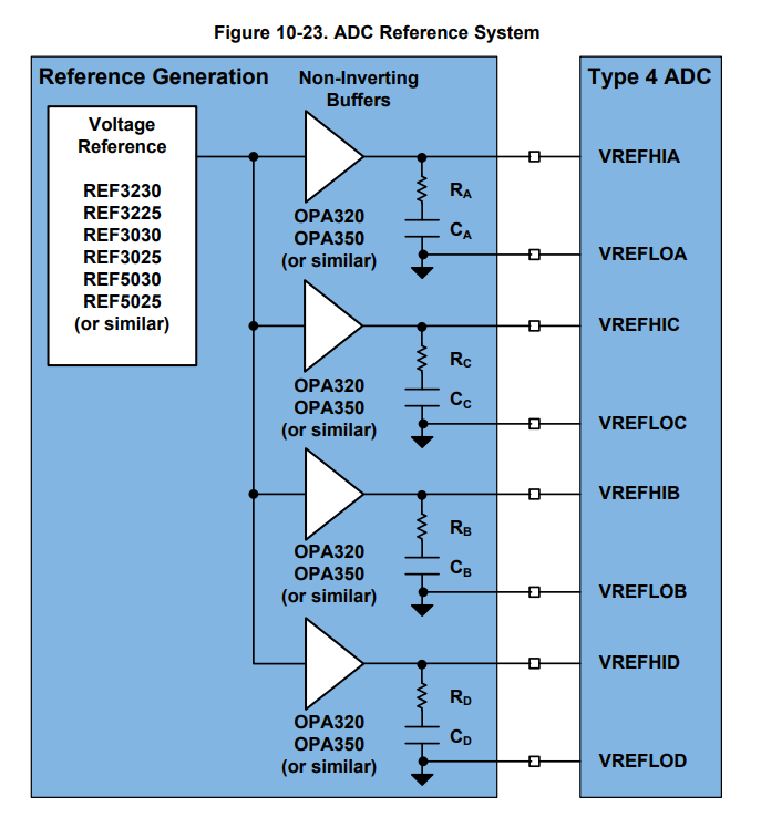
Other Parts Discussed in Thread: CONTROLSUITE, LM4132, OPA320, OPA350, OPA365, LMC6482

Hi,

I am using F28377D silicon revision C on my own custom PCB. I have configured to sample 10 Analog inputs which are distributed to the 3 ADCs (4+3+3). Each Analog input is given through a RC filter to the controller pins,(R - 47 ohms, C - 33pf). while testing, i've shorted all the inputs and given variable voltage by using a Battery and resistive divider network.The ADC clock is configured for 25 MHz and the acquisition window is set to 400 ns in 12 bit single ended mode.Following are the observations.

1.When all the 10 inputs are sampled continuously (using the example software in Controlsuite) , the average value of the results is dropping as the voltage is increased to the full scale 3.3V, and noise of around 150 counts over the average is observed. when a single input  or group of inputs given to a specific ADC are sampled, then the noise counts are reduced to 20.

2.when the group of inputs given to two ADCs are sampled, the noise increased to 150 counts.

3.Then the SOCs are given using Timer1 @16khz frequency for all the ADCs, then the noise counts are reduced to 20,but as in the first case the average value of the results is dropping as the voltage is increased to the full scale 3.3V.when a single input  is sampled, the average value is close to the actual input given.

This behaviour is not improved when i change ADC clock and/or acquisition window.


Please help me to understand what is  happening and suggest whether any proper configurations to be done for ADC.

  • Hi Marada,

    What is the impedance of the voltage divider from your battery? Is there a high speed op-amp buffer after this, before driving into the 47ohm + 33pF network? Usually a battery is not a good test source for an ADC; ideally you should use a good function generator in DC mode with an op-amp locally on the board to decouple the cable impedance. A voltage reference IC + voltage divider + op-amp can also make a good test source.

    What is sourcing the VREFHI voltage? Are the VREFHI capacitors placed right at the VREFHI pin? What is buffering the VREFHI voltage? Are you sure this buffer is stable?

    When you sample the multiple ADCs, are they running in lock-step to meet "synchronous operation"? If not, what package is this?

    We wouldn't expect ADCCLK to help this unless the clock was previously configured above the specified max value of 50MHz. Increasing S+H could potentially help, but only if the source has moderately high impedance; this won't help with very high impedance, noisy input, or a noisy reference.
  • Hi Devin
    The impedance of the voltage divider network is around 2K- 4K ohms and i have not used any opamp buffer .The package of the IC is BGA,all the VREFHI pins of the four ADCs are tied together and the capactiors are placed very near to the Controller. The input to the VREFHI is 3.3V given from Voltage Reference IC LM4132 ,any buffer is not used. The clock and acqps values of all the ADCs are kept same, the synchronous operation was checked by giving the soc triggers using Timer1,does this can ensure synchronous operation?.

    I will check using a voltage reference IC + voltage divider + op-amp.

    Regards,
    Naveen.
  • Hi Naveen,

    So if the divider impedance is 2K followed by 47ohm + 33pF then the input network has an impedance of 2K + 33pF which is an RC time constant of 66ns. You need about 9.7 time constants to settle to 0.25LSBs at 12-bit resolution, so the S+H should be at least 640ns. If you use an op-amp to decouple the divider output from the ADC input then you can use a much shorter S+H (although it will be a little more involved to calculate since you will have to consider the op-amp BW, the external RC, and the internal ADC RC).

    For the reference input, I'm not sure that one LM4132 driving all 4 ADC inputs is going to be great. We typically recommend a high-speed low-noise op-amp to buffer each ADC reference input (although sharing 2 ADC reference between one op-amp output performs well, experimentally). Some good reference drivers are OPA320, OPA350, and OPA365. If this is an issue, reducing the ADCCLK might help. That you see more noise when more ADCs are operating is a symptom that points to inadequate reference bandwidth as a possible culprit.

    Some other things to check based on a quick look through the LM4132 datasheet:
    -maximum stable capacitive load is 10uF. Do you have more capacitance than this between the 4 ADCs?
    -Input capacitance must be greater than output capacitance. If you have ~10uF on the output do you have more than this on the input?

    It sounds like you are good as far as synchronous operation...using CPU Timer as the trigger should work well for this. Also, the BGA package sees less performance degradation when operating the ADCs asynchronously (but it sounds like you are operating them synchronously).
  • Hi Devin,

    I've tried with the voltage reference IC + voltage divider + op-amp as a source for the

    analog inputs and it is working fine with over 10 counts of deviation upto full scale.But for

    the reference pins VREFHI of all ADCs a total of 40MF decoupling capacitance is present.

    As i said earlier,all these pins are shorted and connected to the LM4132. Is this can be a

    problem?


    Regards,

    Naveen.

  • Hi Naveen,

    With a good input signal and reference, it should be possible to get the code spread to about 4 LSBs or so over 256 conversions.  

    One the Reference IC + op-amp side, what ICs are you using?  Do you still have your 47ohm + 33pF capacitor after the op-amp?  Some things you can try here:

    • Increase the 33pF to something in the range of 145pF to 435pF.  This is 10x to 30x the ADC internal S+H capacitor. 
      • You may also want to slightly increase the S+H duration (controlled by ACQPS). Maybe try, 100ns, 150ns, and something really large like 500ns 
    • Add some capacitance at the output of the Reference IC, before the voltage divider.  This can usually be a pretty large amount, maybe 1uF-10uF
    • Add some capacitance at the voltage divider output.  This can be reasonably large, but care must be taken not to destabilize the op-amp.  Probably 100nF to 1uF would be a good choice. 
    • If any of the above uses wires, make them as short as possible and braid them with a ground-return wire.
    • Use an op-amp with higher BW and/or lower noise.  Some good choices would be OPA320, OPA350, or OPA365.       

    For the ADC VREFHI, more capacitance is usually better.  However, the LM4132 has  a maximum capacitive load spec'ed as 10uF, so you could try reducing total capacitance on the pin to this level to see if that helps (either by reducing each capacitor to <2.5uF, or by removing 3 of the 10uF capacitors and only using one ADC - just for debug).  

    The LM4132 datasheet also requires more input capacitance than output capacitance, so you should at least ensure the input has > 40uF of capacitance.  

    However, for best performance each VREFHI pin should be driven by a separate buffer (or at least not driven directly by the reference IC). 

  • Hi Devin,

    The Reference IC used is REF5050, and the OP-amp is LM6482.I still have the RC networks connected in parallel after OP-amp. Actually I've increased the S+H duration to 1.13 Usec. However,still the problem persists when all the ADCs are not run in sync and continuous conversions are configured.I've tried by reducing the output capacitance on LM4132 to 10uF,but of no improvement. Is it really needed to operate all ADCs synchronously??

    Regards,
    Naveen.
  • Hi Marada,

    Since the bandwidth of the LMC6482 is only about ~1MHZ, something in the us range is actually about right for required S+H duration.

    Is the driving circuit constructed on the PCB, or is it a debug setup with physical wires?

    Is a single reference IC + op-amp used to drive all the ADC channels in parallel? I wouldn't be surprised if the kick-back from the ADC sampling is disturbing other channels on a related net (when the ADC S+H opens, there is significant in-rush current as the external capacitance on the pin equalizes with the internal ADC S+H capacitor). Maybe try splitting up the signal sources?

    You could always put a lower quality signal source, like the battery output, on the other channels while you evaluate one input. Then permute the sources and test again, only evaluating the results for op-amp driven channel (but still converting on all the other ADCs for each test).

    If you look at the ADC datasheet specifications, we have degraded specifications for ENOB and ADC-to-ADC isolation when the ADCs are operated asynchronously:

    www.ti.com/.../specifications

    There is also a separate specification for these parameters with the ADCs operating synchronously, which shows no degradation. This is accurate, but this testing used independent reference circuits for each ADC (similar to what is shown in the TRM figure I posted above, which is the recommended reference configuration). If you use a single REFIC, with no buffers, to drive all 4 ADC references, I wouldn't be particularly surprised if you saw some interference via the shared reference path; the reference input is not high impedance, it can be though of as a switched-capacitor type circuit that switches at the beginning of each ADCCLK and needs to be aggressively settled back to the reference voltage by the end of each ADCCLK. This requires a high-bandwidth driver.

    Overall, I think you should look at coupling through the ADC input path first, but if that doesn't get you the performance you want you probably will want to swap-out the reference circuit for the officially recommended configuration.