This thread has been locked.

If you have a related question, please click the "Ask a related question" button in the top right corner. The newly created question will be automatically linked to this question.

TMS320F28069M: temperature dependency and input resistance testing with ADC self calibration

Part Number: TMS320F28069M

Hi,

a customer has some questions on ADC self calibration.

The question is around the F2806x periodic ADC zero offset self calibration required per errata in http://www.ti.com/lit/er/sprz342k/sprz342k.pdf

They are seeing the offset value change somewhat with temperature, where the test setup is spelled out below. Could you let me know if this temperature dependency is to be expected in the range they are seeing below?


Secondly there is a test below that tries to establish dependency on input resistance of the VREFLO path, but I am not sure if this is a good test, please see below. Again is this something within the range expected?


General Setup:

1.       Our system is leveraging the internal voltage reference for the ADC. 

2.       We leave the VREFHI pin floating.

3.       The VREFLO pin is directly shorted to ground.

4.       We run the recommended calibration routine using VREFLO as described on spruh18g p. 499.

5.       The routine for calibration in use ping-pongs between two sets of 5 ADC reads of VREF0, where the first read is discarded, and the 4th read triggers a request for the next set.

6.       A temporary offset of 80 counts is applied and 256 values are accumulated and averaged to find our error.

7.       The routine uses ACQPS = 6 (7 cycles) and no overlap mode is enabled.

8.       *We found that streaming through 8 channels and preserving the first entry did affect the resulting reading generated.


Test setup for ADC offset dependent on temperature

1.       Performing the initialization above sets ADCOFFTRIM to 0x22

2.       We re-run calibration and consistently get this value.

3.       Reading a 1.65V reference reads 0x0822-0x824 (roughly 1.672V).

4.       Nulling the ADCOFFTRIM returns roughly 0x800-0x802

5.       Using another channel and some gain circuitry we applied a 18-24V input and noticed the resulting register value align precisely with the expected input if no offset was applied.

6.       We took out a heat gun and brought the board temperature up from appx 20C to appx 60C.  The voltage range was tested again.  We noticed a possible 1 count drift.  Nothing significant.

7.       We restarted the processor, holding the temperature high.  Calibration generates 0x1E

8.       We re-run calibration, it maintains the new value at temperature.

9.       For each measurement on the ADC, we confirmed the corresponding voltage at the pin with an o-scope with an accuracy of roughly 0.002V


Test setup for ADC offset based on VREFLO input resistance

1.       Setting up a new board, I run a baseline check. Calibration yields 0x1C off VREFLO.

2.       I apply ground to an external pin (B5) and modify the calibration routine to use the external value.  0x1B

3.       I put a 5.9kohm resistor in the way and recalibrate.  0x1D0 (10x the offset).

4.       I replace with a 2.2kohm resistor. 0x13A.

5.       220Ohm, 0x1C4, 0x1C3

6.       10Ohm, 0x18, 0x19, 0x19

7.       3.3Ohm, 0x1D (increasing as we approach 0!)

8.       Floating, 0x16C, 0x16B, 0x167 (Lower than a 5.9k Resistor!)


Conclusions:

1.       There appears to be a strong sensitivity to the input resistance applied to the ADC when a 0V source is applied.

2.       The system naturally appears to relax to 0x167, so it would be natural for resistances above a threshold to approach this value.

3.       For resistance below 500 ohms, the behavior is non-linear.

4.       There is temperature sensitivity in the measurement of a VREFLO.

5.       This sensitivity does not appear to affect ADC readings away from the rails, possibly implying gain error or nonlinearity approaching the rails.

6.       Unsurprisingly, floating values show greater noise in the resulting calibration.

Could someone comment on the tests and conclusions?


Thanks!

--Gunter


  • 1.       There appears to be a strong sensitivity to the input resistance applied to the ADC when a 0V source is applied.

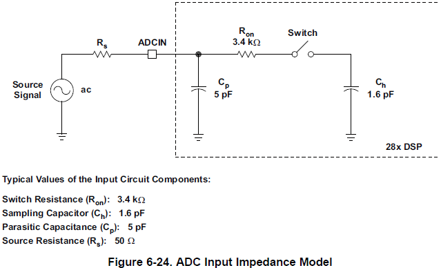
    Additional input resistance (Rs) will slow down the charging time of the ADC sampling capacitor (Ch).  A larger ACQPS value can accommodate the increased resistance.


    2.       The system naturally appears to relax to 0x167, so it would be natural for resistances above a threshold to approach this value. 

    There is no internal biasing of the ADC channels so this "natural" value may be different for each device and channel.

    3.       For resistance below 500 ohms, the behavior is non-linear. 

    Similar to #1, the charging behavior of Ch may appear to be non-linear.

    4.       There is temperature sensitivity in the measurement of a VREFLO. 

    Yes, the ADC offset is expected to drift with temperature, which is why periodic calibration is recommended.

    5.       This sensitivity does not appear to affect ADC readings away from the rails, possibly implying gain error or nonlinearity approaching the rails. 

    Yes, the ADC has gain error specified in the datasheet.  Gain and Offset errors may drift independently of each other.

    6.       Unsurprisingly, floating values show greater noise in the resulting calibration. 

    We consider ADC conversions on floating inputs to be undefined and random in nature.

  • Ignoring the resistance test for now, I would like to focus on the rail to rail linearity and gain calibration concerns.

    We are running Device_cal and the offset calibration routine recommended, with modifications to explicitly address the ADC errata for the first read and the overlapping read corruption.

    The concern here is that on several boards, on several copies of the chip, we found that from the 0x040 to 0x840 count range we were getting consistent measurements between our o-scope on the device pin and the ADC results registers (within about a count) if we did not use the offset calibration routine.

    For values below 0x0040, we see a trend toward the offset calibration, which is why I'm calling out concerns about non-linearity.
    We did not have much testing above 0x840 counts.

    If you believe this is a gain error, spruh18g recommends against modifying the only registers I'm aware of to address gain issues after Device_cal is run.
    How do you recommend we proceed?

    If you believe this is something else, do you see similar behavior on a local test setup?

    We did not see a significant difference between applying ground to an external pin and calibrating vs using VREFLO. 

    We only noted a temperature sensitivity in the offset generated by the calibration routine over temperature.  When we applied no offset, the output values appeared consistent across temperature with ADC readings from roughly 0x040 to 0x840, and from room temperature to 60C applied with a heat gun and measured with an infrared thermometer.  Calibration values generated by the calibration routine on a given board were consistent at a given temperature.

    Do you see similar behavior?

  • Carl Kelso said:

    The concern here is that on several boards, on several copies of the chip, we found that from the 0x040 to 0x840 count range we were getting consistent measurements between our o-scope on the device pin and the ADC results registers (within about a count) if we did not use the offset calibration routine.

    For values below 0x0040, we see a trend toward the offset calibration, which is why I'm calling out concerns about non-linearity.
    We did not have much testing above 0x840 counts.

    If you believe this is a gain error, spruh18g recommends against modifying the only registers I'm aware of to address gain issues after Device_cal is run.
    How do you recommend we proceed?

    If you believe this is something else, do you see similar behavior on a local test setup?

    The following behaviors are expected and checked on every device prior to shipment:

    • When offset calibration is performed, the ADC conversions should converge toward 0 as the input voltage approaches VREFLO.  Gain error can be discounted at this VREFLO floor.  Offset calibration is expected to be the most accurate when it is performed using the same ACQPS settings as the main ADC conversions.
    • As the input voltage approaches the VREFHI ceiling, the gain error becomes the dominant error factor with calibrated offset error becoming negligible.  The gain error may cause the ADC conversions to be clipped at a value less than 4095 at VREFHI, or the conversions may saturate at 4095 before reaching VREFHI.
    • The linearity of the conversions between 0 and MAX ADCRESULT (as determined by the overall gain error) is specified using the DNL and INL parameters.  For example, no more than +/-4 LSBs of INL deviation is expected from the ideal straight line of conversions between 0 and MAX ADCRESULT.

    Can you clarify the behavior of ADCRESULTs trending toward the offset calibration?  What is the ADCRESULT value when sampling VREFLO?

    Does increasing the ACQPS setting help the linearity?  Is the ADC clock configured for 45MHz or less?

    Carl Kelso said:

    We did not see a significant difference between applying ground to an external pin and calibrating vs using VREFLO. 

    We only noted a temperature sensitivity in the offset generated by the calibration routine over temperature.  When we applied no offset, the output values appeared consistent across temperature with ADC readings from roughly 0x040 to 0x840, and from room temperature to 60C applied with a heat gun and measured with an infrared thermometer.  Calibration values generated by the calibration routine on a given board were consistent at a given temperature.

    Do you see similar behavior?

    This sounds like reasonable behavior, but I may be missing a nuanced detail.  The offset calibration is only expected to shift with temperature on a given board.

  • Based on your comments I did some digging. I found that we were setting the ADC clock divider immediately after the offset calibration routine (90MHz != 45MHz). I have moved this to before that function call and the resulting offset is closer to what I would expect (test is 0x50, reading is 0x56).

    I need to rebuild the test setup I used to perform the initial tests, but I will follow up with more information based on this change. The symptoms seem to align, but I would like to confirm that this is the sum of what we are seeing.

    Are there any clocking restrictions like that on device_cal I need to consider as well?
  • Carl,

    As far as I can recall, the clocking quirks primarily apply to the ADC (maximum 45MHz) and supported Flash wait-states.

    -Tommy