This thread has been locked.

If you have a related question, please click the "Ask a related question" button in the top right corner. The newly created question will be automatically linked to this question.

CCS/TMS320F28379D: ADCRESULTx Register question

Part Number: TMS320F28379D


Tool/software: Code Composer Studio

Hello every one! 

I have a problem with a multiple SOC and their results.

I need to use 12 channels, for each channel I use singly SOC. I have started with lunching of one channel, have no problem with this, all works perfect.

The next step was to make 4 SOC for 4 channels, and here the problems begins.

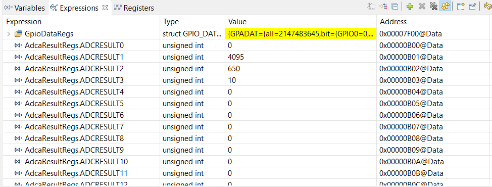
By giving 1.5V at channel A0, I've become result in registers ADCRESULT0 and ADCRESULT1 (See Image 1). 

By giving 1.5V at channel A1, in register ADCRESULT1 (all right).

By giving 1.5V at channel A2, I've become no result at all, and so on.

I have read all examples over 10 times, same thing with Technical Manuals... I have no answers found.

What's a reason could be? 

Thank you!

Image 1

-----------------------------------------------------------------------------------------------------------------------------------------------------------------------------------

//####################################################################
// ePWM1 100 kHz, 50% Duty cycle;
// ePWM1B=!ePWM1A;
// Deadband = 100ns Rising Edge + 100 nS Falling Edge
// PIN49=ePWM1A PIN51=ePWM1B;
// ADC SOC0, CHSEL0 = Pin09
//####################################################################

// Included Files
//
#include "F28x_Project.h"

//
// Defines
//
#define PRD 499 // Period register 2499=20kHz 499=100kHz 99=500kHz
#define DB 20 // Deadband 1 = 10 nS
#define acqps 14 // Acquisition Window 75ns

//
// Globals
//


//
// Function Prototypes
//
void ConfigureADC(void);
void SetupADCEpwm(void);
__interrupt void adca1_isr(void);

void InitEPwm1Example(void);
__interrupt void epwm1_isr(void);


//
// Main
//
void main(void)
{

InitSysCtrl();


// InitGpio();


CpuSysRegs.PCLKCR2.bit.EPWM1=1;

InitEPwm1Gpio();


//
// Configure the ADC and power it up
//
ConfigureADC();
//
// Setup the ADC for ePWM triggered conversions
//
SetupADCEpwm();


DINT;

InitPieCtrl();

IER = 0x0000;
IFR = 0x0000;

InitPieVectTable();


EALLOW; // This is needed to write to EALLOW protected registers
PieVectTable.EPWM1_INT = &epwm1_isr;
PieVectTable.ADCA1_INT = &adca1_isr; //function for ADCA interrupt 1
EDIS; // This is needed to disable write to EALLOW protected registers


EALLOW;
CpuSysRegs.PCLKCR0.bit.TBCLKSYNC = 0;
EDIS;

InitEPwm1Example();

EALLOW;
CpuSysRegs.PCLKCR0.bit.TBCLKSYNC = 1;
EDIS;

IER |= M_INT3;
IER |= M_INT1; //Enable group 1 interrupts
EINT; // Enable Global interrupt INTM
ERTM; // Enable Global realtime interrupt DBGM

PieCtrlRegs.PIEIER3.bit.INTx1 = 1; //PWM
PieCtrlRegs.PIEIER1.bit.INTx1 = 1; //ADC

while(1)
{

} // While end

} // Main end

//////////////////////////////////////////////////////////////////////////////////////////////////////////////////////////////////////////////////

void ConfigureADC(void)
{
EALLOW;

//
//write configurations
//
AdcaRegs.ADCCTL2.bit.PRESCALE = 6; //set ADCCLK divider to /4
AdcSetMode(ADC_ADCA, ADC_RESOLUTION_12BIT, ADC_SIGNALMODE_SINGLE);

//
//Set pulse positions to late
//
AdcaRegs.ADCCTL1.bit.INTPULSEPOS = 1;

//
//power up the ADC
//
AdcaRegs.ADCCTL1.bit.ADCPWDNZ = 1;

//
//delay for 1ms to allow ADC time to power up
//
DELAY_US(1000);

EDIS;
}

void SetupADCEpwm(void)
{
//
//Select the channels to convert and end of conversion flag
//
EALLOW;

AdcaRegs.ADCSOC0CTL.bit.CHSEL = 0; //SOC0 will convert pin A0
AdcaRegs.ADCSOC1CTL.bit.CHSEL = 1; //SOC1 will convert pin A1
AdcaRegs.ADCSOC2CTL.bit.CHSEL = 2; //SOC2 will convert pin A2
AdcaRegs.ADCSOC3CTL.bit.CHSEL = 3; //SOC3 will convert pin A3

AdcaRegs.ADCSOC0CTL.bit.ACQPS = acqps; // 14 = 75ns
AdcaRegs.ADCSOC1CTL.bit.ACQPS = acqps; // 14 = 75ns
AdcaRegs.ADCSOC2CTL.bit.ACQPS = acqps; // 14 = 75ns
AdcaRegs.ADCSOC3CTL.bit.ACQPS = acqps; // 14 = 75ns

AdcaRegs.ADCSOC0CTL.bit.TRIGSEL = 5; //trigger on ePWM1 SOCA
AdcaRegs.ADCSOC1CTL.bit.TRIGSEL = 5; //trigger on ePWM1 SOCA
AdcaRegs.ADCSOC2CTL.bit.TRIGSEL = 5; //trigger on ePWM1 SOCA
AdcaRegs.ADCSOC3CTL.bit.TRIGSEL = 5; //trigger on ePWM1 SOCA

AdcaRegs.ADCINTSEL1N2.bit.INT1SEL = 3; //end of SOC3 will set INT1 flag
AdcaRegs.ADCINTSEL1N2.bit.INT1E = 1; //enable INT1 flag
AdcaRegs.ADCINTFLGCLR.bit.ADCINT1 = 1; //make sure INT1 flag is cleared

EDIS;
}

//
// adca1_isr - Read ADC Buffer in ISR
//
__interrupt void adca1_isr(void)
{

AdcaRegs.ADCINTFLGCLR.bit.ADCINT1 = 1; //clear INT1 flag
PieCtrlRegs.PIEACK.all = PIEACK_GROUP1;
}

//
// epwm1_isr - EPWM1 ISR
//
__interrupt void epwm1_isr(void)
{
//
// Toggle GPIO31 (LED)
//
// GpioDataRegs.GPATOGGLE.bit.GPIO31 = 1 ;
//
// Clear INT flag for this timer
//
EPwm1Regs.ETCLR.bit.INT = 1;

//
// Acknowledge this interrupt to receive more interrupts from group 3
//
PieCtrlRegs.PIEACK.all = PIEACK_GROUP3;
}

//
// InitEPwm1Example - Initialize EPWM1 configuration
//
void InitEPwm1Example()
{
//
// Setup TBCLK
//
EPwm1Regs.TBPRD = PRD; // Set timer period 801 TBCLKs
EPwm1Regs.TBPHS.bit.TBPHS = 0x0000; // Phase is 0
EPwm1Regs.TBCTR = 0x0000; // Clear counter

//
// Set Compare values
//
EPwm1Regs.CMPA.bit.CMPA = PRD/2; // Set compare A value
EPwm1Regs.CMPB.bit.CMPB = 0; // Set Compare B value

//
// Setup counter mode
//
EPwm1Regs.TBCTL.bit.CTRMODE = TB_COUNT_UPDOWN; // Count up and down
EPwm1Regs.TBCTL.bit.PHSEN = TB_DISABLE; // Disable phase loading
EPwm1Regs.TBCTL.bit.HSPCLKDIV = TB_DIV1; // Clock ratio to SYSCLKOUT
EPwm1Regs.TBCTL.bit.CLKDIV = TB_DIV1;

//
// Setup shadowing
//
EPwm1Regs.CMPCTL.bit.SHDWAMODE = CC_SHADOW;
EPwm1Regs.CMPCTL.bit.SHDWBMODE = CC_SHADOW;
EPwm1Regs.CMPCTL.bit.LOADAMODE = CC_CTR_ZERO; // Load on Zero
EPwm1Regs.CMPCTL.bit.LOADBMODE = CC_CTR_ZERO;

//
// Set actions
//
EPwm1Regs.AQCTLA.bit.CAU = AQ_SET; // Set PWM1A on event A, up
// count
EPwm1Regs.AQCTLA.bit.CAD = AQ_CLEAR; // Clear PWM1A on event A,
// down count
EPwm1Regs.AQCTLB.bit.CAU = AQ_CLEAR; // Set PWM1B on event B, up
// count
EPwm1Regs.AQCTLB.bit.CAD = AQ_SET; // Clear PWM1B on event B,
// down count

//
// Active Low PWMs - Setup Deadband
//

EPwm1Regs.DBCTL.bit.OUT_MODE = DB_FULL_ENABLE; // enable Dead-band module
EPwm1Regs.DBCTL.bit.POLSEL = DB_ACTV_HIC; // Active Hi complementary
EPwm1Regs.DBCTL.bit.IN_MODE = DBA_ALL; // ePWMxA - source for Rising-edges, ePWMxB - source for Falling-edges,
EPwm1Regs.DBFED.bit.DBFED = DB;
EPwm1Regs.DBRED.bit.DBRED = DB;

//
// Interrupt where we will change the Compare Values
//
EPwm1Regs.ETSEL.bit.INTSEL = ET_CTR_ZERO; // Select INT on Zero event
EPwm1Regs.ETSEL.bit.INTEN = 1; // Enable INT
EPwm1Regs.ETPS.bit.INTPRD = ET_1ST; // Generate INT on 3rd event

EPwm1Regs.ETSEL.bit.SOCAEN = 1; // Enable SOC on A group
EPwm1Regs.ETSEL.bit.SOCASEL = 4; // Select SOC on up-count
EPwm1Regs.ETPS.bit.SOCAPRD = 1; // Generate pulse on 1st event
}

//
// End of file
//

  • Hi Anton,

    Is your ADC-A INT1 ISR occuring?

    The general setup looks OK: ePWM SOCA triggers ADCA SOC0-SOC3 then end of SOC3 triggers ADCISR.

    The channel select and S+H settings also look OK.

    However, even for A0, it doesn't look like your results are quite rights: even with 3.3V VREFHI range, 1.5V/3.3V*4096 = 1862 but your ADCA result0 is 1699, which is much too low. You might want to check the physical connections for VDDA, VREFHI, and the actual ADC A inputs.

    Is this a TI kit or your own custom board?
  • Hello Devin,
    Yes, adc_interrupt works fine, it's just empty now =)
    I use this Kit www.ti.com/.../TMDSDOCK28379D
    with this ControlCard www.ti.com/.../TMDSCNCD28379D
    so the REFVoltage is intern.
    Besides, most of the time there is another program on this chip, that use ADC and all works fine. And I havn't find distinctions in properties...
    The result from A1 that is laying exactly in ADCRESULT1 show 1863+-5, the same result show result register, when only one channel works. That's meens that there are no problem with REFHI REFLO voltage =(

    I'm stumped... I have even tryed to use the epwm_adc_example but with 4 channels - the same problem.. With one channel even with 4 SOCs all works prety well.
  • Hi Anton,

    I'm also not seeing anything here to explain this.

    Are you using 3.3V = VDDA for the VREFHI or the 3.0V precision reference? (this is selected by a small switch on the control card)

    Is you card revision affected by this erratum and if so have you corrected it?:

    "Warnings about R1.3 of F28379D controlCARD:
    1. R51-R54 were mistakenly populated with 100MΩ resistors instead of 100mΩ resistors. With 100MΩ
    resistors used, the voltage references for the ADCs may not be held adequately constant and the
    accuracy/precision of ADC results may be affected during sampling/conversion. It is recommended that
    customers replace R51-R54 with 100mΩ, 0603, 5% tolerance (or better) resistors. For evaluation of
    the controlCARD in a lab environment, it is also acceptable to short R51-R54 using 0Ω resistors or
    solder bridges; however, populating with 100mΩ is preferred. Please see the following E2E post:
    e2e.ti.com/.../576301 ."
  • Hi Devin,

    thank you for your answer!

    I have checked R51-R54 they are all OK (~100mOhm).

    "In the left position – ADC-A is configured to use VDDA (3.3V) as the ADC’s voltage reference. The fullscale

    range of this ADC will be 0-3.3V, but the ADC will have reduced accuracy/precision.

    • In the right position – ADC-A is configured to either use a precise 3.0V voltage reference or an

    external voltage may be used as a reference. R59 and R60 determine which setting is used (see

    description for R59/R60, above)"

    I am using left position for switches SW2, SW3. This means that the reference voltage is 3.3 V.  

    In previous tests I've applied 1.5 V to A0 channel, this time I've apllied 3.3 V (see screenshot)

    3.3 V to A1

    3.3V to A2

    3.3 V to A3

    It's look like an overflowing is occurring... but why put it the result in others registers? (With 1.5 V same story, but with smaller values)

    Thank you!

  • Hi Anton,

    Are you driving anything on the other channels? In the absence of an input, whatever charge is leftover from previous conversions will be converted.

    It does seem strange that A2 and A3 aren't reading exactly 4095.
  • Hello Devin,
    no, I am using a single cable and applying voltage to each channel separat. 3.3 V I take directly from the Kit-Card.
    In this board another person use his programm with this properties (see code) and ADC works well. I don't need so many interrupts and ADC's only ADCA and one interrupt. I see no difference in properties and don't understand why the result is so wrong...
    ######################################################
    void SetupADC()
    {
    EALLOW;

    //ADC A

    AdcaRegs.ADCSOC0CTL.bit.CHSEL = 0; //SOC0 will convert pin A0
    AdcaRegs.ADCSOC0CTL.bit.ACQPS = ACQ_WINDOW; //sample window
    AdcaRegs.ADCSOC0CTL.bit.TRIGSEL = 5; //trigger on ePWM1 SOCA/C

    // ADC B

    AdcbRegs.ADCSOC1CTL.bit.CHSEL = 2; //SOC0 will convert pin B2
    AdcbRegs.ADCSOC1CTL.bit.ACQPS = ACQ_WINDOW; //sample window
    AdcbRegs.ADCSOC1CTL.bit.TRIGSEL = 5; //trigger on ePWM1 SOCA/C

    AdcbRegs.ADCSOC2CTL.bit.CHSEL = 1; //SOC0 will convert pin B1
    AdcbRegs.ADCSOC2CTL.bit.ACQPS = ACQ_WINDOW; //sample window
    AdcbRegs.ADCSOC2CTL.bit.TRIGSEL = 7; //trigger on ePWM2 SOCA/C

    AdcbRegs.ADCSOC3CTL.bit.CHSEL = 0; //SOC0 will convert pin B0
    AdcbRegs.ADCSOC3CTL.bit.ACQPS = ACQ_WINDOW; //sample window
    AdcbRegs.ADCSOC3CTL.bit.TRIGSEL = 9; //trigger on ePWM3 SOCA/C


    // ADC C

    AdccRegs.ADCSOC4CTL.bit.CHSEL = 2; //SOC0 will convert pin C2
    AdccRegs.ADCSOC4CTL.bit.ACQPS = ACQ_WINDOW; //sample window
    AdccRegs.ADCSOC4CTL.bit.TRIGSEL = 11; //trigger on ePWM4 SOCA/C


    // ADC D

    AdcdRegs.ADCSOC0CTL.bit.CHSEL = 0; //SOC0 will convert pin D0
    AdcdRegs.ADCSOC0CTL.bit.ACQPS = ACQ_WINDOW; //sample window
    AdcdRegs.ADCSOC0CTL.bit.TRIGSEL = 5; //trigger on ePWM1 SOCA/C

    AdcdRegs.ADCSOC1CTL.bit.CHSEL = 1; //SOC0 will convert pin D1
    AdcdRegs.ADCSOC1CTL.bit.ACQPS = ACQ_WINDOW; //sample window
    AdcdRegs.ADCSOC1CTL.bit.TRIGSEL = 5; //trigger on ePWM1 SOCA/C

    AdcdRegs.ADCSOC2CTL.bit.CHSEL = 2; //SOC0 will convert pin D2
    AdcdRegs.ADCSOC2CTL.bit.ACQPS = ACQ_WINDOW; //sample window
    AdcdRegs.ADCSOC2CTL.bit.TRIGSEL = 5; //trigger on ePWM1 SOCA/C

    // Interrupts 1

    AdcbRegs.ADCINTSEL1N2.bit.INT1SEL = 1; //end of SOC1 will set INT1 flag
    AdcbRegs.ADCINTSEL1N2.bit.INT1E = 1; //enable INT1 flag
    AdcbRegs.ADCINTFLGCLR.bit.ADCINT1 = 1; //make sure INT1 flag is cleared

    AdcbRegs.ADCINTSEL1N2.bit.INT2SEL = 2; //end of SOC2 will set INT2 flag
    AdcbRegs.ADCINTSEL1N2.bit.INT2E = 1; //enable INT2 flag
    AdcbRegs.ADCINTFLGCLR.bit.ADCINT2 = 1; //make sure INT1 flag is cleared

    AdcbRegs.ADCINTSEL3N4.bit.INT3SEL = 3; //end of SOC3 will set INT3 flag
    AdcbRegs.ADCINTSEL3N4.bit.INT3E = 1; //enable INT3 flag
    AdcbRegs.ADCINTFLGCLR.bit.ADCINT3 = 1; //make sure INT1 flag is cleared

    // Interrupt 2

    AdccRegs.ADCINTSEL3N4.bit.INT4SEL = 4; //end of SOC4 will set INT4 flag
    AdccRegs.ADCINTSEL3N4.bit.INT4E = 1; //enable INT4 flag
    AdccRegs.ADCINTFLGCLR.bit.ADCINT4 = 1; //make sure INT4 flag is cleared

    EDIS;
    }
  • Hi Anton,

    If you apply the voltage to each channel one-at-a-time (while the other channels are floating) we do expect to see what you presented previously. You need to drive all the channels you are using with some voltage all the time.
  • Hi Devin,

    Thank you for your advice! I will try it and write later an answer =)
  • Hi Devin,

    Your advice was very useful! Now all works pretty good!
    Thank you!

    With best regards,
    Anton