Other Parts Discussed in Thread: ADS127L01
Tool/software: Code Composer Studio
Hi,
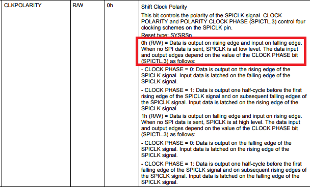
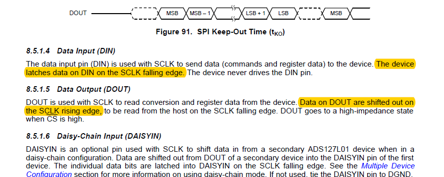
The ADS127L01 ADC if configured for SPI communication works by default with SPI Mode 1 (I know different manufacturers can define it differently, but it latches in on falling and shifts out on rising). Setting CLKPOLARITY bit to 0 and CLOCK PHASE to 0 in f28379D according to the table in datasheet given below should configure it accordingly?
In many cases mode 1 is defined:
"Mode 1: Clock phase is configured such that data is sampled on the falling edge of the clock pulse and shifted out on the rising edge of the clock pulse."
That is wyhy CLKPOLARITY bit to 0 and CLOCK PHASE to 0 should make MCU work in Mode 1. The problem is that the only configuration it works is CLKPOLARITY bit to 1 and CLOCK PHASE to 0. Actually I developed my device and didn't notice this issue since it never caused any problem. I am upgrading some parts of it and came up into that and I am a bit confused.
The ADC requirement is given below:


