This thread has been locked.

If you have a related question, please click the "Ask a related question" button in the top right corner. The newly created question will be automatically linked to this question.

CCS: C28027F Motor Control

Tool/software: Code Composer Studio

Hi all,

I've buit a inverter motor drive using InstaSPIN FOC on a F28027F device.

I've built the inverter stage using a 48-VDC Battery Powered Inverter Power Stage Reference Design for 5-kW Forklift AC Traction Motor Reference Design.

Now I have problem.

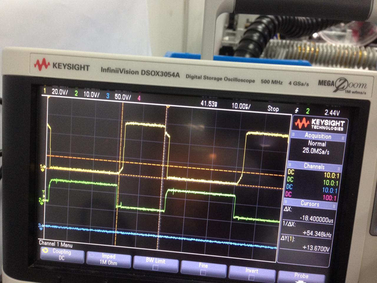
The yellow signal is output of high side gate driver, the green signal is output of low side gate driver.

High side did not turn off quickly.

My question: What is this cause my problem?

Thanks you.

An.

  • This appears to be an issue of the back EMF causing voltage on the line, an effect of the freewheeling diode of the FET. Please also take a scope of the current and back EMF waveforms. If you put them against this plot you should see the correlation there

    Sean
  • Hi Sean,

    Sorry, How to take a scope of the current and back EMF?
  • You can use a current gun probe on one of the phase wires to determine the phase current, and the voltage can be measured across the shunt used to measure phase voltage. That is assuming you use shunt for voltage measurement on your custom hardware

    Sean
  • Hi Sean,

    I will measure late and inform to you. But how to solve this issue?

  • Hi Vu,

    I too have a similar problem on a new design, maybe we can solve it together?   For me I have 310VDC.  My gate switching waveforms are identical to yours, yet despite quite a bit of research and testing I have not been able to find a definitive answer to my issue.

    What you are seeing in your waveform is the turnoff of your upper FET just after the trigger point in your capture. If you put a probe on the source of of the upper mosfet you'll see that little step is the same as your VDC bus + 15V for the gate driver.  When the little step occurs the upper MOSFET should be off because the Vgs is < Vth.

    Now for the interesting part. In my design the the little step is at 310VDC and when the lower FET switches on, that energy has to go somewhere, and it goes into the system in the form of a massive noise spike. I have run my design using Lab1B in open loop mode and disabled the PWM's to all but one channel so as I have a clear view of the system. If you try this you'll see that the MOSFET switching waveforms are the same, regardless if you have an inductive load or not.

    In your waveforms your green channel has spikes. I'm not sure how you have captured this, we solder SMA connectors onto the PCB at the measurement points, or use proper spring type probes as a normal scope ground lead will pickup noise. But if one of those little spikes is > Vth of your MOSFET, it will switch on and smoke will happen.

    What we need to do is work out how to vary the gate resistances or otherwise to limit the effect of switching this energy.

    Here is my scope capture, but I have a 800R load resistor on my phase.  Nevertheless, the amount of energy that gets switched to ground is quite large.

    The two digital lines at the top are the PWM from InstaSPIN, the green is my VCC to the gate driver, yellow is lower gate, pink is upper gate, and blue is the phase voltage (also source pin of upper gate)

    Cheers.

  • Hi Stomp,

    What is gate driver did you user?
    And how many MOSFET parallel for each leg? What value Bootstrap capacitor did you user?
  • Were you able to get the scope measurements that I mentioned earlier in this thread?

    Sean