This thread has been locked.

If you have a related question, please click the "Ask a related question" button in the top right corner. The newly created question will be automatically linked to this question.

TMS320F28379D: About PWM DC cycle-by-cycle action

Part Number: TMS320F28379D

Hi

I'm testing Comparator Ramp generator features for peak current control implementation.
In the program, I use CMPSS1P to compare to ramp value. The result(CMPSS1.CTRIPH) is used
as a DC trip event (cycle-by-cycle) to trip PWM1A to high impedance in the remain part
of the current PWM period.

I found some features are different from what I imaged:

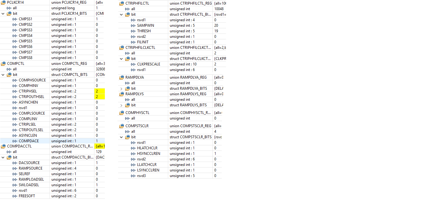
1. I set CMPSS1.COMPCTL[CTRIPHSEL]and CMPSS1.COMPCTL[CTRIPOUTHSEL] to 2, so COMPSTS[COMPHSTS]
will be sent to PWM X-Bar, it will be sent to Output X-Bar (GPIO24) to check this signal.
I think COMPSTS[COMPHSTS] will remain high in a PWM period whenever it becomes high, but when
I check GPIO24, it will become high in a short time then remain low in the subsequent part
of the PWM period. Please see the waveforms below.

My question is why COMPSTS[COMPHSTS] goes low after it becomes high? Do I have any way to
keep COMPSTS[COMPHSTS] high in the remain part of PWM period (except using latched value)?

2. I think in a PWM cycle-by-cycle trip control, when a trip event becomes active, PWM output
will take trip action until the end of the current PWM period. But from above waveforms,
PWM output is only tripped when COMPSTS[COMPHSTS] becomes high and it resumes to normal mode in the
subsequent time of the current PWM period. This is different to type 2 PWM. Do I have any way
to remain trip action at the subsequent time of the current PWM period?

The project is attached for your review.

TestCompRamp1.zip

thanks,

Jiakai

  • Hi Jiakai,

    I haven't looked through your attached project but I think you are seeing this because:
    i. The comparator will trip when the falling ramp crosses the positive input.
    ii. When the trip happens, RAMPMAXREF gets reset to it's predefined value which will untrip the comparator.

    Are you doing up & down count for the epwm? Also can you use the code insertion tool to paste your comparator and epwm configuration code instead of attaching your whole project?
  • Hi Frank,

    Thank you for the information, I know the reason why CMPSS1.CTRIPH/CMPSS1.CTRIPOUTH only
    remains high for a short time. But The issue is: CMPSS1.CTRIPH is used as PWM1 DCAEVT2
    (TRIP4 is active high), PWM1A should take trip action until the end of PWM period when
    CMPSS1.CTRIPH becomes high, but from PWM1A's waveform, it only remains high when CMPSS1.CTRIPH
    is high, and it goes to low when CMPSS1.CTRIPH goes low(see the picture below). Can you find
    any wrong setting at the following initialization code?

    thanks,

    Jiakai

    // Compartor 1 initialization
    EALLOW;
    CpuSysRegs.PCLKCR14.all |= 1; // enable clock to CMPSS1

    Cmpss1Regs.COMPCTL.bit.COMPDACE = 1;
    Cmpss1Regs.COMPHYSCTL.bit.COMPHYS = 0;
    Cmpss1Regs.COMPDACCTL.bit.RAMPSOURCE = 0; // Sync. to PWM1
    Cmpss1Regs.COMPDACCTL.bit.RAMPLOADSEL = 0;
    Cmpss1Regs.COMPDACCTL.bit.SWLOADSEL = 1;
    EDIS;

    // Set Comparator DAC voltage reference
    EALLOW;
    Cmpss1Regs.COMPDACCTL.bit.SELREF = vRef; // use VDDA
    EDIS;

    // Initialize comparator1 high side
    EALLOW;
    Cmpss1Regs.COMPCTL.bit.COMPHSOURCE = 0; // Compare to internal DAC
    Cmpss1Regs.COMPCTL.bit.COMPHINV = 0; // do not invert the result
    Cmpss1Regs.COMPCTL.bit.CTRIPOUTHSEL = 2; // Use digital filter result
    Cmpss1Regs.COMPCTL.bit.CTRIPHSEL = 2; // Use digital filter result
    Cmpss1Regs.COMPCTL.bit.ASYNCHEN = 0;
    Cmpss1Regs.COMPSTSCLR.bit.HSYNCCLREN = 1;
    EDIS;

    // Set digital filter, window:0.2us, 95%
    EALLOW;
    Cmpss1Regs.CTRIPHFILCLKCTL.bit.CLKPRESCALE = 2;
    Cmpss1Regs.CTRIPHFILCTL.bit.THRESH = 19; // 19 of 20
    Cmpss1Regs.CTRIPHFILCTL.bit.SAMPWIN = 20;
    Cmpss1Regs.CTRIPHFILCTL.bit.FILINIT = 1;
    EDIS;

    // Initialize Ramp generator
    EALLOW;
    Cmpss1Regs.COMPDACCTL.bit.DACSOURCE = 1; // use ramp
    EDIS;
    Cmpss1Regs.RAMPDLYS.bit.DELAY = 0;
    Cmpss1Regs.RAMPDECVALS = 2;


    // Pwm X-Bar initialization: CMPSS1.CTRIPH as TRIP4 input
    EALLOW;
    EPwmXbarRegs.TRIP4MUX0TO15CFG.all &= ~0x3UL;
    EPwmXbarRegs.TRIP4MUX0TO15CFG.all |= 0; // Set CMPSS1.CTRIPH as TRIP4 input
    EPwmXbarRegs.TRIP4MUXENABLE.all |= 1; // enable that mux input
    EDIS;

    // Pwm X-Bar TRIP4: do not invert
    EALLOW;
    EPwmXbarRegs.TRIPOUTINV.all &= ~1UL; // do not invert
    EDIS;

    // Output X-Bar initialization: CMPSS1.CTRIPOUTH as OUTPUT1 input
    EALLOW;
    OutputXbarRegs.OUTPUT1MUX0TO15CFG.all &= ~0x3UL;
    OutputXbarRegs.OUTPUT1MUX0TO15CFG.all |= 0; // Set CMPSS1.CTRIPH as OUTPUT1 input
    OutputXbarRegs.OUTPUT1MUXENABLE.all |= 1; // enable that mux input
    EDIS;

    // Output1 initialization
    EALLOW;
    OutputXbarRegs.OUTPUTINV.all &= ~1; // do not invert
    OutputXbarRegs.OUTPUTLATCHENABLE.all &= ~1; // do not use latch
    EDIS;

    // Set GPIO24 for Output X-Bar OUTPUT2
    ...

    // PWM1 initialization
    EALLOW;
    CpuSysRegs.PCLKCR2.all |= 1; // Enable PWM1 clock
    EDIS;
    EPwm1Regs.TBCTL.all = 0x0000;
    EPwm1Regs.TBCTL.bit.CTRMODE = TB_COUNT_UP;
    EPwm1Regs.TBCTR = 0x0000;
    // Set GPIO0/GPIO1 to PWM
    // Set PWM1A action mode
    EPwm1Regs.AQCTLA.all = 0x0000;
    EPwm1Regs.AQCTLB.all = 0x0000;
    EPwm1Regs.AQCTLA.bit.ZRO = AQ_SET; // for up count sawtooth
    EPwm1Regs.AQCTLA.bit.CAU = AQ_CLEAR;
    // Set PWM1B as complementary of PWM1A
    EPwm1Regs.AQCTLB.bit.ZRO = AQ_CLEAR; // for up count sawtooth
    EPwm1Regs.AQCTLB.bit.CAU = AQ_SET;
    EALLOW;
    EPwm1Regs.HRCNFG.all = 0; // Reset HRPWM setting
    EDIS;

    // Set PWM1 dead band
    EPwm1Regs.DBCTL.all = 0;
    EPwm1Regs.DBCTL.bit.HALFCYCLE = 1;
    EPwm1Regs.DBCTL.bit.IN_MODE = 0; // PWMxA as the source of rising edge and PWMxA as the source of falling edge
    EPwm1Regs.DBCTL.bit.POLSEL = dbType;
    EPwm1Regs.DBCTL.bit.OUT_MODE = 0x03;
    EPwm1Regs.DBRED.bit.DBRED = 0;
    EPwm1Regs.DBFED.bit.DBFED = 0;

    // Set PWM1 interrupt type
    EPwm1Regs.ETPS.bit.INTPSSEL = 1;
    EPwm1Regs.ETINTPS.bit.INTPRD2 = 1;
    EPwm1Regs.ETSEL.bit.INTSEL = 0x004; // int on CMPA/C up count
    EPwm1Regs.ETSEL.bit.INTSELCMP = 1; // use CMPC
    EPwm1Regs.CMPC = 0; // Set interrupt position to the beginning of PWM period.

    // Set PWM1 interrupt vector
    EALLOW;
    PieVectTable.EPWM1_INT = Task;
    PieCtrlRegs.PIEACK.all = PIEACK_GROUP3;
    PieCtrlRegs.PIEIER3.all |= 1;
    IER |= M_INT3;
    EPwm1Regs.ETCLR.bit.INT = 1;
    EPwm1Regs.ETSEL.bit.INTEN = 1;
    EDIS;

    // Set PWM1 trip action
    EALLOW;
    EPwm1Regs.TZCTL2.bit.ETZE = 0;
    EPwm1Regs.TZCTL.bit.TZB = 1; // force high to PWM1B
    EPwm1Regs.TZCTL.bit.DCBEVT1 = 1; // force high to PWM1B
    EPwm1Regs.TZCTL.bit.DCBEVT2 = 1; // force high to PWM1B
    EPwm1Regs.TZCTL.bit.TZA = 2; // force low to PWM1A
    EPwm1Regs.TZCTL.bit.DCAEVT1 = 2; // force low to PWM1A
    EPwm1Regs.TZCTL.bit.DCAEVT2 = 2; // force low to PWM1A
    EDIS;

    // Start PWM1
    EALLOW;
    EPwm1Regs.TZCLR.bit.OST = 1;
    EDIS;

    // Set DC event
    EALLOW;
    EPwm1Regs.DCAHTRIPSEL.all = 8;
    EPwm1Regs.DCALTRIPSEL.all = 0;
    EPwm1Regs.DCTRIPSEL.bit.DCAHCOMPSEL = 0xF;
    EPwm1Regs.DCTRIPSEL.bit.DCALCOMPSEL = 0xF;
    EPwm1Regs.TZDCSEL.bit.DCAEVT2 = 2;
    EPwm1Regs.DCTRIPSEL.all = 0xFFFF;
    EDIS;

    // PS_PwmSetDcEvtFilter
    EALLOW;
    EPwm1Regs.DCACTL.bit.EVT1SRCSEL = 1;
    EPwm1Regs.DCFCTL.bit.SRCSEL = dcFltApply;
    EPwm1Regs.DCFCTL.bit.BLANKE = 0;
    EDIS;

    // DAC innitialization
    EALLOW;
    CpuSysRegs.PCLKCR16.all |= 1UL << 16; // enable clock to module
    DacaRegs.DACCTL.bit.SYNCSEL = 0; // Set Sync. PWM to PWM1
    DacaRegs.DACCTL.bit.LOADMODE = 1;
    DacaRegs.DACOUTEN.bit.DACOUTEN = 1; // enable DAC output
    EDIS;

    // Set DAC voltage reference to
    EALLOW;
    DacaRegs.DACCTL.bit.DACREFSEL = 1; // Set DAC-A's voltage reference to ADC VREFHI/VREFLO
    EDIS;

    // Start PWM1 clock
    EALLOW;
    CpuSysRegs.PCLKCR0.bit.TBCLKSYNC = 1; // Enable TBCLK after all ePWM setting
    EDIS;

  • Jiakai,

    I don't see RAMPMAXREFS being configured in your code. Is this configured somewhere else?
  • Hi Frank,

    RAMPMAXREFS is not set at initialization function, it is set to 2.0v in function Task() as follows:

    fVDC3 = 2.0;
    fZOH1 = fVDC3;
    CMP_RAMPMAXREF(1) = fZOH1 * (65535.0/3.3);

    CMP_RAMPMAXREF is defined as below:
    #define CMP_RAMPMAXREF(ch) *((Uint16 *)(0x5C6A + 0x20 * ch))
    // ch: 1, 2 or 3

    thanks,
    Jiakai
  • Jiakai,

    Ok. I noticed you are using a lot of macro functions which might not always expand to what you expect. So before looking into this any further, can you confirm in the CCS watch window that all the registers are programmed to what you expect?
  • Hi Frank,

    I have made some minor changes on the initialization code, it doesn't affect PWM actions.

    The new code is as follows:

    // Compartor 1 initialization
    EALLOW;
    CpuSysRegs.PCLKCR14.all |= 1; // enable clock to CMPSS1

    Cmpss1Regs.COMPCTL.bit.COMPDACE = 1;
    Cmpss1Regs.COMPHYSCTL.bit.COMPHYS = 0;
    Cmpss1Regs.COMPDACCTL.bit.RAMPSOURCE = 0; // Sync. to PWM1
    Cmpss1Regs.COMPDACCTL.bit.RAMPLOADSEL = 0;
    Cmpss1Regs.COMPDACCTL.bit.SWLOADSEL = 1;
    EDIS;

    // Set Comparator DAC voltage reference
    EALLOW;
    Cmpss1Regs.COMPDACCTL.bit.SELREF = 0; // use VDDA
    EDIS;

    // Initialize comparator1 high side
    EALLOW;
    Cmpss1Regs.COMPCTL.bit.COMPHSOURCE = 0; // Compare to internal DAC
    Cmpss1Regs.COMPCTL.bit.COMPHINV = 0; // do not invert the result
    Cmpss1Regs.COMPCTL.bit.CTRIPOUTHSEL = 2; // Use digital filter result
    Cmpss1Regs.COMPCTL.bit.CTRIPHSEL = 2; // Use digital filter result
    Cmpss1Regs.COMPCTL.bit.ASYNCHEN = 0;
    Cmpss1Regs.COMPSTSCLR.bit.HSYNCCLREN = 1;
    EDIS;

    // Set digital filter, window:0.2us, 95%
    EALLOW;
    Cmpss1Regs.CTRIPHFILCLKCTL.bit.CLKPRESCALE = 2;
    Cmpss1Regs.CTRIPHFILCTL.bit.THRESH = 19; // 19 of 20
    Cmpss1Regs.CTRIPHFILCTL.bit.SAMPWIN = 20;
    Cmpss1Regs.CTRIPHFILCTL.bit.FILINIT = 1;
    EDIS;

    // Initialize Ramp generator
    EALLOW;
    Cmpss1Regs.COMPDACCTL.bit.DACSOURCE = 1; // use ramp
    EDIS;
    Cmpss1Regs.RAMPDLYS.bit.DELAY = 0;
    Cmpss1Regs.RAMPDECVALS = 2;


    // Pwm X-Bar initialization: CMPSS1.CTRIPH as TRIP4 input
    EALLOW;
    EPwmXbarRegs.TRIP4MUX0TO15CFG.all &= ~0x3UL;
    EPwmXbarRegs.TRIP4MUX0TO15CFG.all |= 0; // Set CMPSS1.CTRIPH as TRIP4 input
    EPwmXbarRegs.TRIP4MUXENABLE.all |= 1; // enable that mux input
    EDIS;

    // Pwm X-Bar TRIP4: do not invert
    EALLOW;
    EPwmXbarRegs.TRIPOUTINV.all &= ~1UL; // do not invert
    EDIS;

    // Output X-Bar initialization: CMPSS1.CTRIPOUTH as OUTPUT1 input
    EALLOW;
    OutputXbarRegs.OUTPUT1MUX0TO15CFG.all &= ~0x3UL;
    OutputXbarRegs.OUTPUT1MUX0TO15CFG.all |= 0; // Set CMPSS1.CTRIPH as OUTPUT1 input
    OutputXbarRegs.OUTPUT1MUXENABLE.all |= 1; // enable that mux input
    EDIS;

    // Output1 initialization
    EALLOW;
    OutputXbarRegs.OUTPUTINV.all &= ~1; // do not invert
    OutputXbarRegs.OUTPUTLATCHENABLE.all &= ~1; // do not use latch
    EDIS;

    // Set GPIO24 for Output X-Bar OUTPUT2
    ...

    // PWM1 initialization
    EALLOW;
    CpuSysRegs.PCLKCR2.all |= 1; // Enable PWM1 clock
    EDIS;
    EPwm1Regs.TBCTL.all = 0x0000;
    EPwm1Regs.TBCTL.bit.CTRMODE = TB_COUNT_UP;
    EPwm1Regs.TBCTR = 0x0000;
    // Set GPIO0/GPIO1 to PWM
    // Set PWM1A action mode
    EPwm1Regs.AQCTLA.all = 0x0000;
    EPwm1Regs.AQCTLB.all = 0x0000;
    EPwm1Regs.AQCTLA.bit.ZRO = AQ_SET; // for up count sawtooth
    EPwm1Regs.AQCTLA.bit.CAU = AQ_CLEAR;
    // Set PWM1B as complementary of PWM1A
    EPwm1Regs.AQCTLB.bit.ZRO = AQ_CLEAR; // for up count sawtooth
    EPwm1Regs.AQCTLB.bit.CAU = AQ_SET;
    EALLOW;
    EPwm1Regs.HRCNFG.all = 0; // Reset HRPWM setting
    EDIS;

    // Set PWM1 dead band
    EPwm1Regs.DBCTL.all = 0;
    EPwm1Regs.DBCTL.bit.HALFCYCLE = 1;
    EPwm1Regs.DBCTL.bit.IN_MODE = 0; // PWMxA as the source of rising edge and PWMxA as the source of falling edge
    EPwm1Regs.DBCTL.bit.POLSEL = 2;
    EPwm1Regs.DBCTL.bit.OUT_MODE = 0x03;
    EPwm1Regs.DBRED.bit.DBRED = 0;
    EPwm1Regs.DBFED.bit.DBFED = 0;

    // Set PWM1 interrupt type
    EPwm1Regs.ETPS.bit.INTPSSEL = 1;
    EPwm1Regs.ETINTPS.bit.INTPRD2 = 1;
    EPwm1Regs.ETSEL.bit.INTSEL = 0x004; // int on CMPA/C up count
    EPwm1Regs.ETSEL.bit.INTSELCMP = 1; // use CMPC
    EPwm1Regs.CMPC = 0; // Set interrupt position to the beginning of PWM period.

    // Set PWM1 interrupt vector
    EALLOW;
    PieVectTable.EPWM1_INT = Task;
    PieCtrlRegs.PIEACK.all = PIEACK_GROUP3;
    PieCtrlRegs.PIEIER3.all |= 1;
    IER |= M_INT3;
    EPwm1Regs.ETCLR.bit.INT = 1;
    EPwm1Regs.ETSEL.bit.INTEN = 1;
    EDIS;

    // Set PWM1 trip action
    EALLOW;
    EPwm1Regs.TZCTL2.bit.ETZE = 0;
    EPwm1Regs.TZCTL.bit.TZB = 1; // force high to PWM1B
    EPwm1Regs.TZCTL.bit.DCBEVT1 = 1; // force high to PWM1B
    EPwm1Regs.TZCTL.bit.DCBEVT2 = 1; // force high to PWM1B
    EPwm1Regs.TZCTL.bit.TZA = 2; // force low to PWM1A
    EPwm1Regs.TZCTL.bit.DCAEVT1 = 2; // force low to PWM1A
    EPwm1Regs.TZCTL.bit.DCAEVT2 = 2; // force low to PWM1A
    EDIS;

    // Start PWM1
    EALLOW;
    EPwm1Regs.TZCLR.bit.OST = 1;
    EDIS;

    // Set DC event
    EALLOW;
    EPwm1Regs.DCAHTRIPSEL.all = 8; // Select TRIPINPUT4
    EPwm1Regs.DCALTRIPSEL.all = 0; // do not use
    EPwm1Regs.DCTRIPSEL.bit.DCAHCOMPSEL = 0xF; // allow trip combination
    EPwm1Regs.DCTRIPSEL.bit.DCALCOMPSEL = 0xF; // allow trip combination
    EPwm1Regs.TZDCSEL.bit.DCAEVT2 = 2; // DCAH active high
    EDIS;

    // PS_PwmSetDcEvtFilter
    EALLOW;
    EPwm1Regs.DCACTL.bit.EVT1SRCSEL = 1;
    EPwm1Regs.DCFCTL.bit.SRCSEL = 2;
    EPwm1Regs.DCFCTL.bit.BLANKE = 0;
    EDIS;

    // DAC innitialization
    EALLOW;
    CpuSysRegs.PCLKCR16.all |= 1UL << 16; // enable clock to module
    DacaRegs.DACCTL.bit.SYNCSEL = 0; // Set Sync. PWM to PWM1
    DacaRegs.DACCTL.bit.LOADMODE = 1;
    DacaRegs.DACOUTEN.bit.DACOUTEN = 1; // enable DAC output
    EDIS;

    // Set DAC voltage reference to
    EALLOW;
    DacaRegs.DACCTL.bit.DACREFSEL = 1; // Set DAC-A's voltage reference to ADC VREFHI/VREFLO
    EDIS;

    // Start PWM1 clock
    EALLOW;
    CpuSysRegs.PCLKCR0.bit.TBCLKSYNC = 1; // Enable TBCLK after all ePWM setting
    EDIS;

    I have also checked all register values, they are same as the code set (except the value of

    Cmpss1Regs.CTRIPHFILCTL.bit.FILINIT is 0, but I think it is cleared by CPU).

    I took some register snapshots as below,

    thank you very much!

    Jiakai


  • Hi Jiakai,

    Thanks for posting the register screenshots. I think your problem is coming from not configuring TZSEL. You will need to configure TZSEL to choose the source for CBC. Please look at the "Trip-Zone Submodule Mode Control Logic" diagram in the TRM to see what i mean. It also looks like you have a few conflicting settings in your code for the trip zone. It's recommended to set any non-actions to "do nothing". Let us know if that helps.
  • Hi Frank,

    I added TZSEL to the program, it works.

    Thank you very much,

    Jiakai

  • Glad to hear it's working now! Let us know if you ran into anymore issues.