This thread has been locked.

If you have a related question, please click the "Ask a related question" button in the top right corner. The newly created question will be automatically linked to this question.

CCS/TIEVM-HV-1PH-DCAC: Inverter compensation coding

Part Number: TIEVM-HV-1PH-DCAC

Tool/software: Code Composer Studio

Hello.
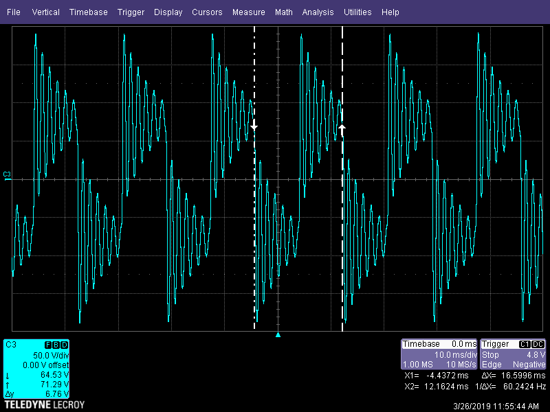
I am exploring compensation behavior using the TIEVM-HV-1PH-DCAC demo board.
I code the demonstration source as equally as possible, but the output oscillates.
I set the PWM, ADC, and compensation parameters the same.
I am analyzing for more than one week, but it is difficult for me to work on compensation myself for the first time.

The source code was saved using Project> Export> General> Archive File.
I hope you will take a look at the source code.

I need your support.

Thank you.


myInverter_1phase.zip

  • "I code the demonstration source as equally as possible, but the output oscillates.
    I set the PWM, ADC, and compensation parameters the same."

    Can you please be more specific on the problem you faced? Can you also attach some pics on what you set in the compensation designer and what is the output?

    Thank you.

    Regards,

    Chen

  • memory data.xlsx

    Thank you for your comment.

    The compensation parameter value is used by copying the value of the demo source code.

    Attachment is an Excel file that investigated memory in the open loop state for infVoRefInst (Sine Reference), ADC_VLINE_VOLT (Inverter output voltage measurement data), and ADC_VHALL_VOLT (Product current measurement data).

    I hope this helps you with your analysis.

    The contents of myDCL.h file of the attached element code are as follows.

    //myDCL.h header file
    #define KPV_1H        		0.5
    #define KIV_1H        		2000
    #define WRCV_1H        		0.00628
    #define KIV_3H        		1000
    #define WRCV_3H        		0.031415
    #define KIV_5H        		1000
    #define WRCV_5H        		0.031415
    #define KIV_7H        		500
    #define WRCV_7H        		0.031415
    
    #define PI_KP 0.5093949150
    #define PI_KI 0.0812101701
    
    #define GI_A1 -1.0000000000
    #define GI_A2 0.0000000000
    #define GI_A3 0.0000000000
    #define GI_B0 0.5467500000
    #define GI_B1 -0.4252500000
    #define GI_B2 0.0000000000
    #define GI_B3 0.0000000000
    #define GI_MAX 1.0
    #define GI_MIN -1.0
    
    #define GV_LEAD_LAG_A1 -0.8789881828
    #define GV_LEAD_LAG_A2 0.0000000000
    #define GV_LEAD_LAG_B0 4.3590034523
    #define GV_LEAD_LAG_B1 -4.2308212342
    #define GV_LEAD_LAG_B2 0.0000000000
    #define GV_LEAD_LAG_IMIN -1.0
    #define GV_LEAD_LAG_MAX 1.0
    #define GV_LEAD_LAG_MIN -1.0
    
    // DF22
    DCL_DF22 gi = DF22_DEFAULTS;
    DCL_PI pie = PI_DEFAULTS;
    float32_t gi_out;
    
    // DF22
    DCL_DF22 gv_pr1 = DF22_DEFAULTS;
    DCL_DF22 gv_r3 = DF22_DEFAULTS;
    DCL_DF22 gv_r5 = DF22_DEFAULTS;
    DCL_DF22 gv_r7 = DF22_DEFAULTS;
    DCL_DF22 gv_r9 = DF22_DEFAULTS;
    DCL_DF22 gv_r11 = DF22_DEFAULTS;
    DCL_DF22 gv_lead_lag = DF22_DEFAULTS;
    float32_t gv_out;
    float32_t gv_lead_lag_out;
    
    //TODO computeDF22_PRcontrollerCoeff(
    void computeDF22_PRcontrollerCoeff(DCL_DF22 *v, float32_t kp, float32_t ki,
                                       float32_t wo, float32_t fs, float32_t wrc )
    {
        float32_t temp1, temp2, wo_adjusted;
        wo_adjusted=2*fs*tan(wo/(2*fs));
    
        temp1=4*fs*fs+wo_adjusted*wo_adjusted+4*fs*wrc;
        temp2=4*ki*wrc*fs/temp1;
        v->b0=temp2;
        v->b1=0;
        v->b2=-temp2;
        v->a1=((-8*fs*fs+2*wo_adjusted*wo_adjusted)/temp1);
        v->a2=((temp1-8*fs*wrc)/temp1);
        v->x1=0;
        v->x2=0;
    
        if(kp!=0)
        {
            v->b0+=kp;
            v->b1+=kp*v->a1;
            v->b2+=kp*v->a2;
        }
    
        v->a1=(v->a1);
        v->a2=(v->a2);
    }
    
    void dcl_config(void)
    {
    	float32 woV;
    	woV = 2.0*PI*OUT_FREQ;
    	computeDF22_PRcontrollerCoeff(&gv_pr1, KPV_1H, KIV_1H, woV, PWM_FREQ, WRCV_1H);
    	woV = 2.0*PI*OUT_FREQ * 3;
    	computeDF22_PRcontrollerCoeff(&gv_r3 , 0     , KIV_3H, woV, PWM_FREQ, WRCV_3H);
    	woV = 2.0*PI*OUT_FREQ * 5;
    	computeDF22_PRcontrollerCoeff(&gv_r5 , 0     , KIV_5H, woV, PWM_FREQ, WRCV_5H);
    	woV = 2.0*PI*OUT_FREQ * 7;
    	computeDF22_PRcontrollerCoeff(&gv_r7 , 0     , KIV_7H, woV, PWM_FREQ, WRCV_7H);
    
    	gi.a1 = (float32)(GI_A1);
    	gi.a2 = (float32)(GI_A2);
    	gi.b0 = (float32)(GI_B0);
    	gi.b1 = (float32)(GI_B1);
    	gi.b2 = (float32)(GI_B2);
    	gi.x1 = 0;
    	gi.x2 = 0;
    
    	// PI coefficients
    	pie.Kp= (float) (PI_KP);
    	pie.Ki= (float) (PI_KI);
    
    	gv_lead_lag.a1=(float)(GV_LEAD_LAG_A1);
        gv_lead_lag.a2=(float)(GV_LEAD_LAG_A2);
        gv_lead_lag.b0=(float)(GV_LEAD_LAG_B0);
        gv_lead_lag.b1=(float)(GV_LEAD_LAG_B1);
        gv_lead_lag.b2=(float)(GV_LEAD_LAG_B2);
        gv_lead_lag.x1=0;
        gv_lead_lag.x2=0;
    
    }


    The ADC settings are shown below.

    //myADC.h header file
    void adc_config(void)
    {
        ADC_VBUS_CNT = 0;
        ADC_VBUS_RMS_HEX = 0;
        ADC_CNT = 0;
    
        EALLOW;
        //ADCA - VBus : CH5
        AdcaRegs.ADCCTL2.bit.PRESCALE = 6;                                      
        AdcSetMode(ADC_ADCA, ADC_RESOLUTION_12BIT, ADC_SIGNALMODE_SINGLE);     
        AdcaRegs.ADCCTL1.bit.INTPULSEPOS = 1;                                   
        AdcaRegs.ADCCTL1.bit.ADCPWDNZ = 1;                                      
    
        //ADCB - Current Hall Sensor : CH2
        AdcbRegs.ADCCTL2.bit.PRESCALE = 6;
        AdcSetMode(ADC_ADCB, ADC_RESOLUTION_12BIT, ADC_SIGNALMODE_SINGLE);
        AdcbRegs.ADCCTL1.bit.INTPULSEPOS = 1;
        AdcbRegs.ADCCTL1.bit.ADCPWDNZ = 1;
    
        //ADCC - VLine(Inverter Output) : CH14
        AdccRegs.ADCCTL2.bit.PRESCALE = 6;
        AdcSetMode(ADC_ADCC, ADC_RESOLUTION_12BIT, ADC_SIGNALMODE_SINGLE);
        AdccRegs.ADCCTL1.bit.INTPULSEPOS = 1;
        AdccRegs.ADCCTL1.bit.ADCPWDNZ = 1;
    
        AdcaRegs.ADCSOC0CTL.bit.CHSEL = 5;          //Vbus use SOC0                           
        AdcaRegs.ADCSOC0CTL.bit.ACQPS = 31;                                   
        AdcaRegs.ADCSOC0CTL.bit.TRIGSEL = 5;                                   
    
        AdcbRegs.ADCSOC0CTL.bit.CHSEL = 2;        //Current Hall Sensor use SOC0, SOC1, SOC2, SOC3
        AdcbRegs.ADCSOC0CTL.bit.ACQPS = 31;
        AdcbRegs.ADCSOC0CTL.bit.TRIGSEL = 5;
    
        AdcbRegs.ADCSOC1CTL.bit.CHSEL = 2;
        AdcbRegs.ADCSOC1CTL.bit.ACQPS = 31;
        AdcbRegs.ADCSOC1CTL.bit.TRIGSEL = 5;
        AdcbRegs.ADCSOC2CTL.bit.CHSEL = 2;
        AdcbRegs.ADCSOC2CTL.bit.ACQPS = 31;
        AdcbRegs.ADCSOC2CTL.bit.TRIGSEL = 5;
        AdcbRegs.ADCSOC3CTL.bit.CHSEL = 2;
        AdcbRegs.ADCSOC3CTL.bit.ACQPS = 31;
        AdcbRegs.ADCSOC3CTL.bit.TRIGSEL = 5;


        AdccRegs.ADCSOC0CTL.bit.CHSEL = 14;        //VLine use SOC0
        AdccRegs.ADCSOC0CTL.bit.ACQPS = 31;
        AdccRegs.ADCSOC0CTL.bit.TRIGSEL = 5;
    
    //do not use interrupt // AdccRegs.ADCINTSEL1N2.bit.INT1SEL = 0; // AdccRegs.ADCINTSEL1N2.bit.INT1E = 1; // AdccRegs.ADCINTFLGCLR.bit.ADCINT1 = 1; DELAY_US(1000); //1ms Delay EDIS; }

    //ADC Calibration Code

    //myADC.h header file
    #define ADC_VLINE_382V_HEX		4095
    #define ADC_VLINE_0V_HEX		2244
    #define ADC_VLINE_N382V_HEX		393
    #define ADC_VLINE_CAL_VOLT		(float32)382.17				
    #define ADC_VLINE_REF_HEX		(ADC_VLINE_382V_HEX - ADC_VLINE_0V_HEX)	
    float32 ADC_VLINE_VOLT;		//Inverter Output Measurement value
    
    #define ADC_VBUS_410V_HEX		4095		
    #define ADC_VBUS_CAL_VOLT		(float32)410.6888361
    float32 ADC_VBUS_VOLT;           //Input DC source Measurement value
    
    
    #define ADC_VHALL_972A_HEX		4095		//9.72085A Max
    #define ADC_VHALL_0A_HEX		2266		//0A
    #define ADC_VHALL_N972A_HEX		437			//-9.72085A Max
    #define ADC_VHALL_CAL_CURR		(float32)9.72085				
    #define ADC_VHALL_REF_HEX		(ADC_VHALL_972A_HEX - ADC_VHALL_0A_HEX)
    float32 ADC_VHALL_VOLT;         //Current Hall Sensor Measurement Value
    
    //Return : Inverter output measurement value
    //Range : +1 ~ -1 , +1(382.17Vpk) -1(-382.17Vpk)
    void adc_vline_calc(int16 adc_hex) { ADC_VLINE_VOLT = (float32)(adc_hex - ADC_VLINE_0V_HEX) / ADC_VLINE_REF_HEX; }
    //Return : Input DC source measurement value
    //Range : 0 ~ +1 , 0(0Vdc) +1(410.68Vdc) void adc_vbus_calc(Uint16 adc_hex) { ADC_VBUS_VOLT = (float32)adc_hex / ADC_VBUS_410V_HEX; } //Return : Current Hall Sensor output measurement value
    //Range : -1 ~ +1 , +1(9.72Apk) -1(-9.72Apk) void adc_vhall_calc(Uint16 adc_hex0, Uint16 adc_hex1, Uint16 adc_hex2, Uint16 adc_hex3) { ADC_VHALL_VOLT = (float32)((float32)(adc_hex0 + adc_hex1 + adc_hex2 + adc_hex3) * 0.25 - ADC_VHALL_0A_HEX) / ADC_VHALL_REF_HEX; //이값은 100% 단위로 계산된 값이다. }


    The PWM settings are shown below.

    //myPWM.h Header file
    void epwm1_epwm2_config(void)
    {
        EALLOW;
        //Step1. PWM1 Config
        EPwm1Regs.TBCTL.bit.PRDLD = 0;                      
        EPwm1Regs.TBPRD = ((Uint16)(PWM_PERIOD) >> 1);    //100MHz / 20kHz / 2 = 2500
        EPwm1Regs.TBCTR = 0;                                
        EPwm1Regs.TBPHS.bit.TBPHS = 0;                      
        EPwm1Regs.TBCTL.bit.CTRMODE = 2;                
        EPwm1Regs.TBCTL.bit.CLKDIV = 0;                     
        EPwm1Regs.TBCTL.bit.HSPCLKDIV = 0;             
    
        EPwm1Regs.CMPA.bit.CMPA = 0;                        
        EPwm1Regs.CMPCTL.bit.SHDWAMODE = 0;    
        EPwm1Regs.CMPCTL.bit.LOADAMODE = 0;     
    
        EPwm1Regs.AQCTLA.bit.CAU = 2;       
        EPwm1Regs.AQCTLA.bit.CAD = 3;       
        EPwm1Regs.AQCTLA.bit.ZRO = 1;       
    
        EPwm1Regs.DBCTL.bit.HALFCYCLE = 0;         
        EPwm1Regs.DBRED.bit.DBRED = PWM_DEAD_BAND;   
    
        EPwm1Regs.DBFED.bit.DBFED = PWM_DEAD_BAND;
        EPwm1Regs.DBCTL.bit.IN_MODE = 0;                  
        EPwm1Regs.DBCTL.bit.POLSEL = 2;                    
        EPwm1Regs.DBCTL.bit.OUT_MODE = 3;              
    
        EPwm1Regs.TBCTL.bit.PHSEN = 0;                      
        EPwm1Regs.TBCTL.bit.SYNCOSEL = 1;               
    
    
        //Step2. PWM2 Config
        EPwm2Regs.TBCTL.bit.PRDLD = 0;
        EPwm2Regs.TBPRD = ((uint16_t)(PWM_PERIOD) >> 1);
        EPwm2Regs.TBCTR = 0;
        EPwm2Regs.TBPHS.bit.TBPHS = 0;                     
        EPwm2Regs.TBCTL.bit.CTRMODE = 2;
        EPwm2Regs.TBCTL.bit.CLKDIV = 0;
        EPwm2Regs.TBCTL.bit.HSPCLKDIV = 0;
    
        EPwm2Regs.CMPA.bit.CMPA = 0;
        EPwm2Regs.CMPCTL.bit.SHDWAMODE = 0;                
        EPwm2Regs.CMPCTL.bit.LOADAMODE = 0;
    
        EPwm2Regs.AQCTLA.bit.CAD = 1;                     
    
        EPwm2Regs.DBCTL.bit.HALFCYCLE = 0;
        EPwm2Regs.DBRED.bit.DBRED = PWM_DEAD_BAND;
        EPwm2Regs.DBFED.bit.DBFED = PWM_DEAD_BAND;
        EPwm2Regs.DBCTL.bit.IN_MODE = 0;
        EPwm2Regs.DBCTL.bit.POLSEL = 2;
        EPwm2Regs.DBCTL.bit.OUT_MODE = 3;
    
        EPwm2Regs.TBCTL.bit.PHSEN = 1;
        EPwm2Regs.TBCTL.bit.SYNCOSEL = 0;            
        EPwm2Regs.TBCTL.bit.PHSDIR = 1;                  
    
        EPwm1Regs.ETSEL.bit.SOCASEL = 6;					
        EPwm1Regs.CMPB.bit.CMPB = EPwm1Regs.TBPRD - (32 << 1);	//32 eqal  ADC's ACQPS sampling time
    
        EPwm1Regs.ETPS.bit.SOCPSSEL = 1;					
        EPwm1Regs.ETSOCPS.bit.SOCAPRD2 = 1;				
    
        EPwm1Regs.ETSEL.bit.SOCAEN = 1;					
    
        //Interrupt setting
        EPwm1Regs.ETSEL.bit.INTSEL = 2;						//TBCTR = PRD
        EPwm1Regs.ETPS.bit.INTPSSEL = 1;
        EPwm1Regs.ETINTPS.bit.INTPRD2 = 1;
        EPwm1Regs.ETSEL.bit.INTEN = 1;
        EPwm1Regs.ETCLR.bit.INT = 1;
        EDIS;
    
    
        //Step3. GPIO0(PWM1A), 1(PWM1B), 2(PWM2A), 3(PWM2B) 설정
        EALLOW;
        GpioCtrlRegs.GPADIR.bit.GPIO0 = 1;                  
        GpioCtrlRegs.GPADIR.bit.GPIO1 = 1;
        GpioCtrlRegs.GPADIR.bit.GPIO2 = 1;
        GpioCtrlRegs.GPADIR.bit.GPIO3 = 1;
    
        GpioCtrlRegs.GPAPUD.bit.GPIO0 = 0;                 
        GpioCtrlRegs.GPAPUD.bit.GPIO1 = 0;
        GpioCtrlRegs.GPAPUD.bit.GPIO2 = 0;
        GpioCtrlRegs.GPAPUD.bit.GPIO3 = 0;
    
        GpioCtrlRegs.GPAMUX1.bit.GPIO0 = 1;               
        GpioCtrlRegs.GPAMUX1.bit.GPIO1 = 1;               
        GpioCtrlRegs.GPAMUX1.bit.GPIO2 = 1;               
        GpioCtrlRegs.GPAMUX1.bit.GPIO3 = 1;               
        EDIS;
    }


    //Zero dection and pwm resetting
    void pwm_zero_cross_dection(void)
    {
    	if(sine_direct_prev != sine_direct)		// π -> 2π -> π change event occured?
    	{
    		sine_direct_prev = sine_direct;
    		if(sine_direct) //0~180 degrees
    		{
    			EPwm1Regs.AQCTLA.bit.CAU = 2;
    			EPwm1Regs.AQCTLA.bit.CAD = 3;
    			EPwm1Regs.AQCTLA.bit.ZRO = 1;
    			EPwm2Regs.AQCTLA.bit.CAD = 1;
    		}
    		else //180 ~ 360 degrees
    		{
    			EPwm1Regs.AQCTLA.bit.CAU = 1;
    			EPwm1Regs.AQCTLA.bit.CAD = 3;
    			EPwm1Regs.AQCTLA.bit.ZRO = 2;
    			EPwm2Regs.AQCTLA.bit.CAD = 2;
    		}
    	}
    }
    

    Interrupt Service Routine are  shown below.

    //myInterrupt.h header file
    
    interrupt void pwm1_isr(void)
    {
    	static float32 err, invVoRef, invVoRefInst, invDutyPU, gv_out, gv_lead_lag_out, gi_out;
    
            //Return(ADC_VBUS_VOLT) input dc voltage measurement value ( 0 ~ 1)
    	adc_vbus_calc(AdcaResultRegs.ADCRESULT0);
            
            //Return(ADC_VLINE_VOLT) ouput ad voltage measurement value (-1 ~ +1)
    	adc_vline_calc(AdccResultRegs.ADCRESULT0);
    
            //Return(ADC_VHALL_VOLT) current hall sensor measurement value (-1 ~ +1)
    	adc_vhall_calc(AdcbResultRegs.ADCRESULT0, AdcbResultRegs.ADCRESULT1, AdcbResultRegs.ADCRESULT2, AdcbResultRegs.ADCRESULT3);
    
        sine_calc();		//Return (sine_out)  , 0(0deg) -> 1(90deg) -> 0(180deg) -> -1(270deg) -> 0(360deg)
    
        invVoRef = VOUT_RMS_SET;	       // VOUT_RMS_SET : Setting Gain - Enter a value between 0 and 1
        invVoRefInst = sine_out * invVoRef;  
    
        err = invVoRefInst - ADC_VLINE_VOLT;
    
    	gv_out= DCL_runDF22_C1(&gv_pr1, err)
    			+ DCL_runDF22_C1(&gv_r3, err)
    			+ DCL_runDF22_C1(&gv_r5, err)
    			+ DCL_runDF22_C1(&gv_r7, err);
    
    	gv_lead_lag_out= DCL_runDF22_C1(&gv_lead_lag, gv_out);
    
        gi_out = DCL_runDF22_C1(&gi, (gv_lead_lag_out - ADC_VHALL_VOLT));
    
    /////////////////// Open Loop Control //////////////
    //    invDutyPU = invVoRefInst;
    /////////////////////////////////////////////////////////////////
    
    ///////////////// /Close Loop control ////////////////
        invDutyPU = (gi_out + ADC_VLINE_VOLT) / ADC_VBUS_VOLT;
    /////////////////////////////////////////////////////////////////
    	invDutyPU= (invDutyPU>(float)(0.98))?(float)(0.98):invDutyPU;
    	invDutyPU= (invDutyPU<(float)(-0.98))?(float)(-0.98):invDutyPU;
    
    //PWM CMPA setting
        EPwm1Regs.CMPA.bit.CMPA = (float32)2500 * (1-fabs(invDutyPU));
    //    EPwm1Regs.CMPA.bit.CMPA = EPwm1Regs.TBPRD - ((float32)(EPwm1Regs.TBPRD) * fabs(invDutyPU));
        if(EPwm1Regs.CMPA.bit.CMPA == EPwm1Regs.TBPRD) EPwm1Regs.CMPA.bit.CMPA = 2499;
        EPwm2Regs.CMPA.bit.CMPA = 1;
    
    //Zero crossing detection
        pwm_zero_cross_dection();
    
    
        EPwm1Regs.ETCLR.bit.INT = 1;        //Interrupt Flag Clear
        PieCtrlRegs.PIEACK.all = PIEACK_GROUP3;
    }
    

    sine_calc() function are shown below.

    //mySine.h header file

    #define PI          3.141592654
    #define PI2         6.283185307
    #define FREQ_STEP    (float32)(PWM_FREQ / OUT_FREQ)      
    #define PI2_STEP     (float32)(PI2 / FREQ_STEP)          
    
    void sine_calc(void)
    {
    	if((sine_gain > 1) || (sine_gain < 0)) sine_gain = 1;
        sine_out = sin(sine_step_now) * sine_gain;
    
        if(sine_step_now <= PI ) sine_direct = 1;        //Positive 0~180
        else sine_direct = 0;                            //Negative 181~360
    
        sine_step_now = sine_step_now + PI2_STEP;
        if(sine_step_now >= PI2)
        {
        	sine_direct_pi2 = 1;						
            sine_step_now = sine_step_now - PI2;
        }
    }
    

    Below is the inverter output waveform when open loop.

    Below is the inverter output waveform when close loop.

    When press RUN in Debug mode, a vibration waveform is instantly generated.
    VOUT_RMS_SET is initialized to 0.0 and Bus DC input voltage is 40Vdc.
    And there is no load.

    This is the waveform when the bus input voltage is raised to 80V under the above conditions.

    At this time, the bus input current increased to 0.29A, and the voltage could not be raised anymore.

    Please help me.
    Thank you.

  • Hi Sir.
    I have not been able to solve it yet.
    I have tried SDFM for a few days, but the symptoms are the same.
    I think I missed some parts, please help.
    Have a good day~
  • Hi,

    1. Is the board the same as TIEVM-HV-1PH-DCAC?

    2. Looks like you took sections of the code and pasted it into your project? 

    3. When you say loop is closed is it the current loop? we follow an inner current with outer voltage loop method to tune the VSI mode?

    4. I am assuming you are testing VSI?

    5. Please patiently read the UG and understand the code, there is no substitute to that, 

  • You're right.

    There was a problem throughout the process of converting the original source code to the modern style.

    Currently, the Voltage close loop and current close loop and Grid connection have been tested.
    I'd like to ask you some advice in the Grid connection experiment, and I'm going to ask you a new question.
    Thank you for your interest and for your reply.