This thread has been locked.

If you have a related question, please click the "Ask a related question" button in the top right corner. The newly created question will be automatically linked to this question.

TIEVM-VIENNARECT: VIENNA rectifier communication lights are not bright:A:D3 and A:D4,I dont know if the hardware question or it need configure,can anyone help me?

Part Number: TIEVM-VIENNARECT
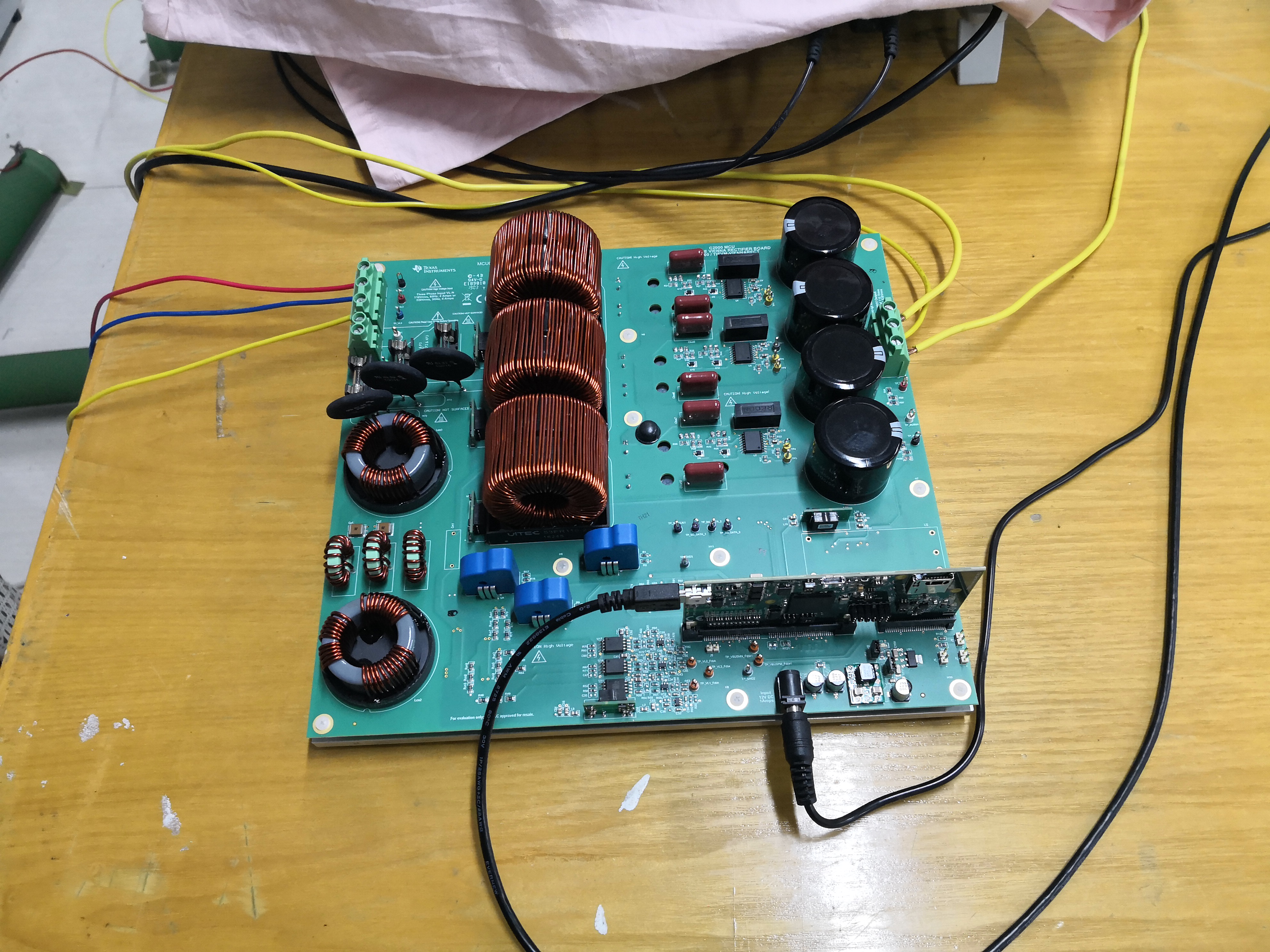
Other Parts Discussed in Thread: SFRA, TIDM-1007, TIDM-1000

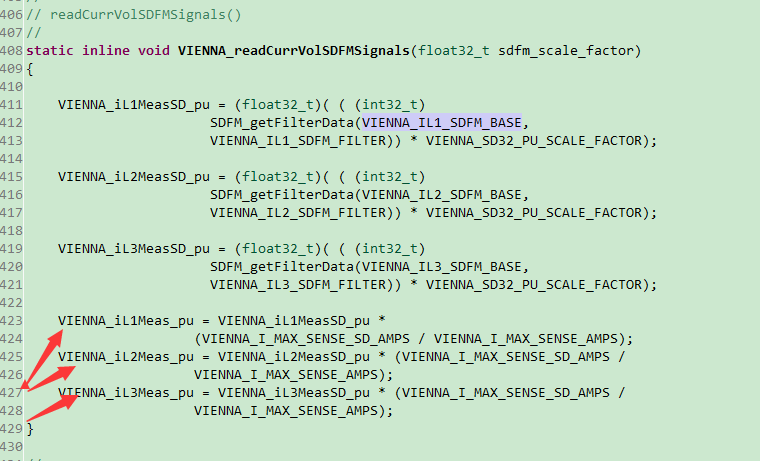
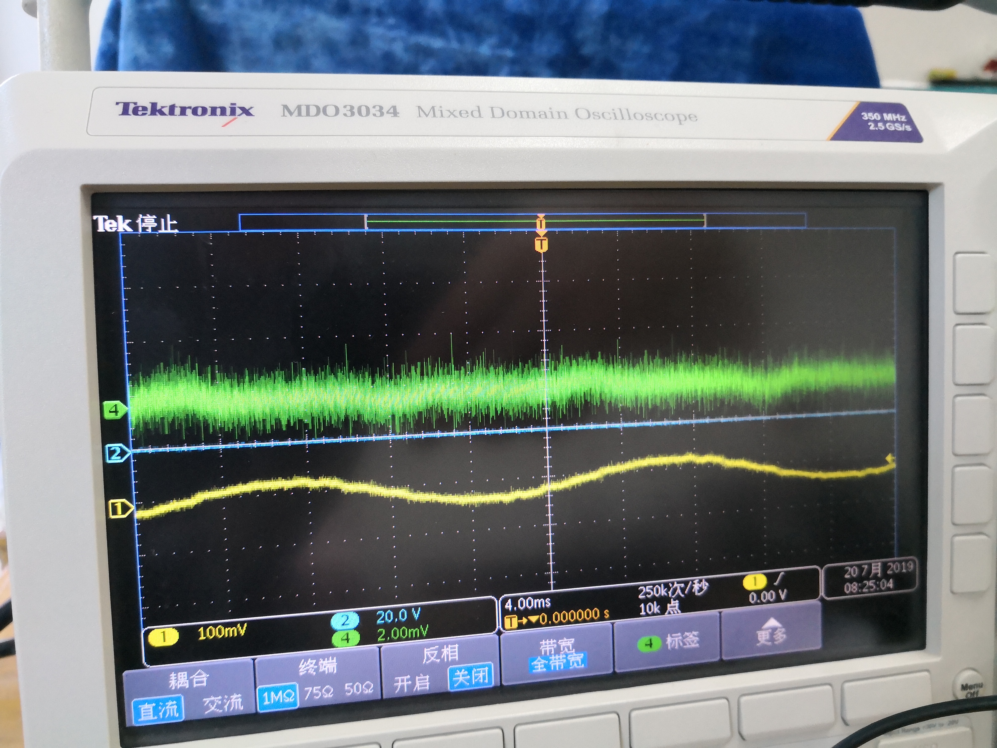
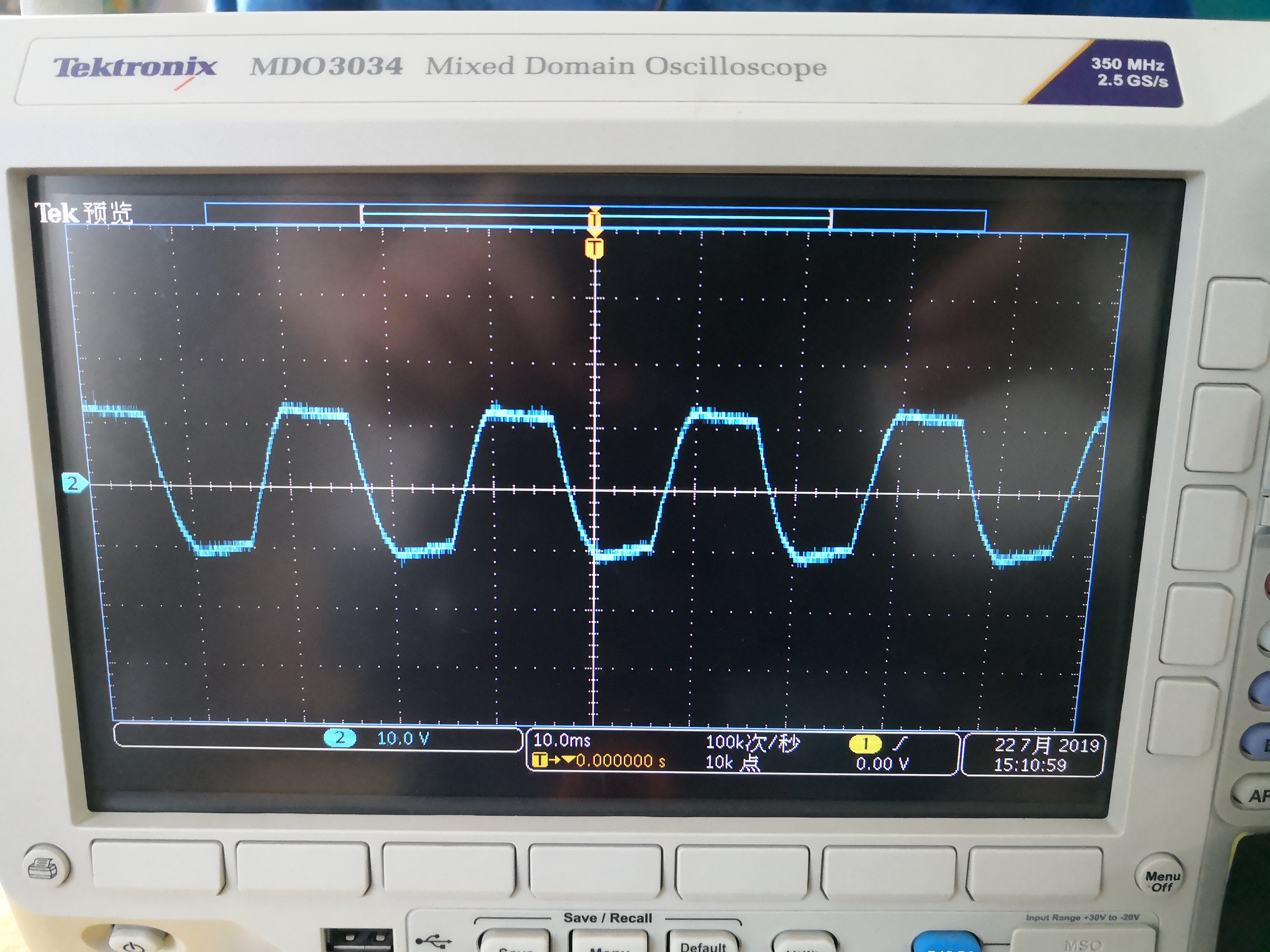
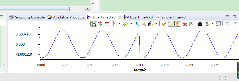
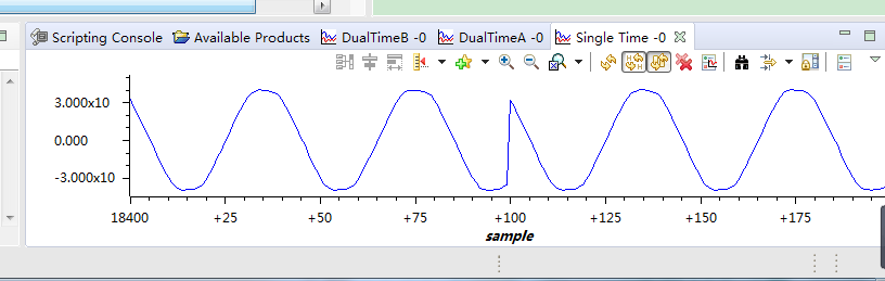
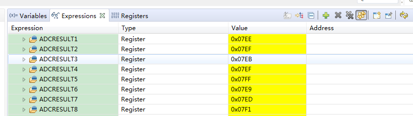
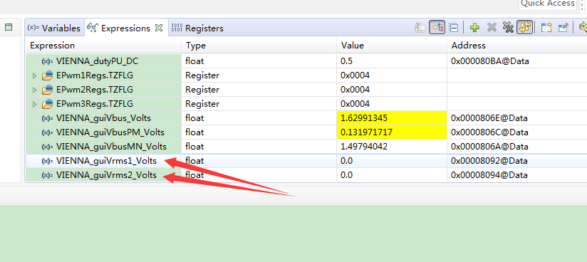
and  V1,V2,V3 I1,I2,I3 ,the voltage and current of variable window is not update in time,as the figure below.

  • Hi,

    1. A:D3 and A:D4 will only toggle when the SFRA GUI is connected.

    2. If you increase the input voltage to more than 20 ~ 30V, you will start to see those parameters updating. 

    Regards,

    Chen

  • 1.The input voltage is more than 50V,but Vrms2 and Vrms3 Still not updated.The value of Vrms1 shown above is the same as that shown by the oscilloscope, but the value measured by the multimeter is less than ten volts. What's the matter?

    2.And I set all the switches of Sw2 and Sw3 to the left, and A: SW1 to the top, right?

    3.The Dual time graphs are unavailable,as shown  in the following figure. I did it step by step according to the guides.

  • Hi,

    1.The input voltage is more than 50V,but Vrms2 and Vrms3 Still not updated.The value of Vrms1 shown above is the same as that shown by the oscilloscope, but the value measured by the multimeter is less than ten volts. What's the matter?

    If the scope matches the value in the expressing window, it is good for me. I don't know what happened for your multimeter measurement. Those two should match for the RMS value.

    If Vrms1 is updating means the ISR is working, can you go back to check the ADC sensing values(not the GUI value, the initial ADC value) of Vrms2 and Vrms3? If they are both 0, then you need to check the hardware connection and settings. If not, then there are something wrong in the code. But if you have not changed the code, the software should work correctly.

    2.And I set all the switches of Sw2 and Sw3 to the left, and A: SW1 to the top, right?

    Which device are you using? please refer to the control card settings of user guide which should give you the correct settings. If it is f2837x, then it is correct.

    3.The Dual time graphs are unavailable,as shown in the following figure. I did it step by step according to the guides.

    According to the errors, it seems like the start address is not set correctly. They should be &dBuff1 and  &dBuff2.


    Let me know if that helps. Thanks.


    Regards,

    Chen

  • As shown above,this problem Still in existence:Start address,cannot evaluate address

    2.here,ISR code pfccontrolcode have twp functions,readcurvolADCsignals() and readcurvolSDFMSignals(). VIENNA_il1MeasSD_PU,VIENNA_il2MeasSD_PU,VIENNA_il3MeasSD_PU,Should their values follow the previous function or the latter?

    3.When the input voltage has not increased, the value of Vrms1 has reached 22V. The input voltage has increased. Vrms2 and Vrms3 are still not updated. I don't know what to do. Is there something wrong with hardware or software?What should I do?I did exactly what the manual said.

  • i,

    Which device are you using? if it is f2837x, please add "BUILD_F2837XD" as a predefined symbol. You can add it by right click the project in CCS and click property, then extend "build", "C2000 compiler" and "predefined symbol". This should help you solve the missing updating parameter issue. This is just to give you a workaround, and we will update the solution soon.

    For the dual time graph, please directly enter "VIENNA_dBuff1" or "VIENNA_dBuff2".. as the address. Please do not use the file to create the settings directly. This is due to the parameter name change. We are going to update the file and user guide in the future.

    Sorry for the inconvience.

    Regards,

    Chen

  • 1.The input voltage is shown in the figure below. Is that right?


    2.The input voltage is normal, but the A phase current is problematic.The last one is A phase current(Green).Is it possible that there is a problem with my three-phase input AC source?


  • Hi,

    1. It is correct, but you probably can try to tune the acquisition size and the display data size to make it better.

    2.The current waveforms are correct. Is that the waveform of phase one current? I have not seen this issue before and I believe it is not something in the code, but according to the value shown in the expression window, it is huge (16.75 A?). Have you changed the original code other than the suggestion I gave to you? It can be something wrong with the Board or the AC source. Can you directly measure the three phase current in the oscilloscope to make sure the value shown in the CCS is correct? 

    Regards,

    Chen 

  • Answer your second question. The current value of iL1 is not updated in real time. Its value is wrong and the actual input is not that large.

    1.

    As shown above,As shown in the figure above, the input currents of three phases a, B and C are normal, which proves that there are problems in hardware or internal code. I have never modified the code. In the expression window, the current values of phase A are not updated in real time, it always keep the value of -1.39A, and other values can be updated normally. What's the matter? What should I do? The last figure is a fixed duty cycle. Is his waveform correct? The waveforms of the six pins on the board I tested are exactly the same as this one.

    2.As shown in the pictures above,they are a and b phase circuit,Why are waveforms not continuous? There is a vertical line between them.

  • Hi,

    1. 

    For the debug purpose, please change the settings in vienna_settings.h as below:

    from #define VIENNA_SDFM_SENSING 1 

    to #define VIENNA_SDFM_SENSING 0 

    I notice that VIENNA_iL1Meas_pu is not updating, can you enter the "AdcaResultRegs" in the expression window? and check whether ADCresult0~11 are updating? can you please attach a pic of that to me as before?

    Are all the three phase current you measured using oscilloscope or multimeter showing the correct value?  Can you also probe the IL1 sensing signal to see if it is correct?

    It is not like a software issue for me, more of a hardware sensing issue.

    2.  Please try to set acquisition size and the display data size both to 100.

    Regards,

    Chen

  • 1.According to what you said, current and voltage waveforms can be displayed normally, and all values can be updated normally, but what is the value of Adcresult 0-11 not decimal?

    2.The last figure is the fixed duty cycle under the open loop. The yellow one is TP6 pin and the blue one is Tp5 pin. Why are these two waveforms not inverted? They came from the same way, didn't they?

  • Sorry, I'm not uploading a graph.This is phase A. Compared with the oscilloscope diagram, it comes in a, B and C order.

    I hope you can see it clearly.

  • for the graph tool, please use the settings below:

    But keep in mind you need to change the address accordingly based on your interest

  • For the PWM output, please take a look at page 7,  and there are some notes as below:

    Though Q1 and Q2 are shown to be not switching here for understanding, the current flow does not change even when it is switched. SW for TIDM-1007 switches the FETs synchronously with each other

  • 1.When should I set define VIENNA_SDFM_SENSING to 1?In the previous reply, you asked me to set it to 0.

    2.Can I continue the experiment of the second part current closed loop now?

    3.Though Q1 and Q2 are shown to be not switching here for understanding, the current flow does not change even when it is switched. SW for TIDM-1007 switches the FETs synchronously with each other。

    I don't quite understand the meaning of this sentence.As shown in the figure below, aren't PWM1A and PWM1B waveforms complementary? Aren't the waveforms tested by Tp5 and Tp6 ?Can you explain it for me?

  • 1. You can always set VIENNA_SDFM_SENSING to 0.

    2. Do all the parameters value show up correctly? If yes, than you can jump into the next build

    3. The picture showing up in the user guide is one solution to setup the PWM. However, we implement the PWM in another way which is the waveform you saw in the scope. The PWM 1 and 2 are the same. They are not inverted. The notes is just to explain why this implementation can still work. 

    Thanks.

    Regards,

    Chen

  • 1.SDFM module is used for filtering, isn't it?Isn't the waveform effect better after filtering?I wonder know if I can use SDFM module properly.

    2.Can epwm output in-phase or in-phase waveforms by setting them? As shown above, in the cases of 2 and 4, only one tube is conducting. Aren't their waveforms complementary?

  • Today, I have done some experiments on closed-loop current. Here are a few questions I would like to ask you.

    1.The input voltage is 30V,DC side voltage is 70V. When I clear PWM trip,DC side voltage increase to 140V,Circuit boards emit louder current sounds. I see the guide manual whose DC side voltage reaches 600V,I don't have courage to try such a large voltage,because I am afraid that in case of hardware damage, it will affect my next experiment. Can I continue to validate the voltage loop at the input voltage of 30V?

    2.Can I test other  algorithmic experiments in the present baseboard ?
    3.What model is the double-loop setting in the guide based on? Do you have any relevant reference papers? I think the guide only briefly introduces them. I don't understand them. Generally, the PI double closed-loop control I come into contact with is based on DQ coordinates.

    4.I still can't understand why the duty cycle should be set in the same phase. The duty cycle waveform I tested under the current loop today is still the same phase.

    5.Is there a schematic diagram of  the 28379D control board of the Autium designer version ? Can you send it to me?

    Thank you,Looking forward to  your reply.

  • To answer your first two questions:

    1. SDFM is used as another sensing way like ADC. You can set value back to 1 and it should be fine to use the SDFM.

    2. The key idea is to create the current flow path no matter it is through the MOSFET or the body diode. So both settings are ok. Means it can be complementary or "on and off" at the same time.

    Regards,

    Chen

  • 1.The input voltage is 30V,DC side voltage is 70V. When I clear PWM trip,DC side voltage increase to 140V,Circuit boards emit louder current sounds. I see the guide manual whose DC side voltage reaches 600V,I don't have courage to try such a large voltage,because I am afraid that in case of hardware damage, it will affect my next experiment. Can I continue to validate the voltage loop at the input voltage of 30V?

    No, the best way to do it is to follow the user guide. Always make sure all the parameters in the express window make sense. Please do not jump to the next build until you fully verify the current build. Do not always run it with 30V input. Also please check the current protection and voltage protection under build 1 and set appropriate values. Some noise is expected but should not be too loud.  

    2.Can I test other  algorithmic experiments in the present baseboard ?

    Yes, you can theoretically. But all the other experiments should be done carefully by yourself because if is out of our reference design.

    3.What model is the double-loop setting in the guide based on? Do you have any relevant reference papers? I think the guide only briefly introduces them. I don't understand them. Generally, the PI double closed-loop control I come into contact with is based on DQ coordinates.

    We don't have any other reference, but your can search for the related reference online. For motor control, it is usually like that as you mentioned.

    4.I still can't understand why the duty cycle should be set in the same phase. The duty cycle waveform I tested under the current loop today is still the same phase.

    It is true in our code they are "on and off",  that is the reason we have those notes there. 

    5.Is there a schematic diagram of  the 28379D control board of the Autium designer version ? Can you send it to me?

    please initial another thread for this question so that we can better assist you because it is not directly related to TIDM-1000.

    Thanks.

    Chen

  • HEllo,

    1.Would you like to put the baseboard directly on the wooden table? Need not take any heat dissipation measures?Or I'll find something to support it.?

    2.F2837X_180controlCARD_R1_3 is the latest Schematic diagram?Does this schematic have an Altium disigner version?can you send me?

    3.In the guide handbook, the DC side is connected with 500 ohms resistance. Can I connect only one resistor of 10 kW and 200 ohms? Because I don't have a resistance of 500 euros here. I have a couple of 1kw, 50Euro resistors here. Can you give me any viable solutions?

    regards,

    JIa

  • Hi,

    1. That is fine as long as you do not run above the power level mentioned in the user guide. There is already a heat sink below.

    2.Please create another thread for this question so that we can better assist you.

    3. No, you can't do it by using the original code because the output voltage is fixed and the power level(listed in the first page of the user guide) will be too high. I will suggest to use the 500 ohms or some resistor close to that value.

    Regards,

    Chen

  • Hi, 

    I notice you create another thread so I will go ahead to close this one since the problem has been solved. Thanks.

    Regards,

    Chen