Part Number: DRV8302-HC-C2-KIT
Other Parts Discussed in Thread: CONTROLSUITE
Hi every one,
I have been working on DRV8302-HC-C2-KIT with ti\controlSUITE\development_kits\DRV830x-HC-C2-KIT_v105\InstaSPIN_BLDC project. My main goal is sensorless trapezoidal control of BLDC motor.
Although it is working fine with example code, I failed when I tried to get meaningful values from ADC channel, i mean DC bus current.
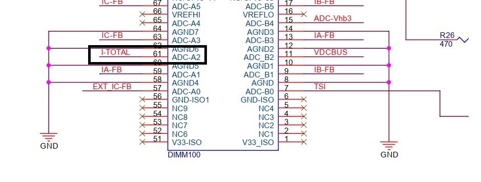
In this project, DC bus current is reading through ADC-A2 as can be seen below.
and also I initialized ADC with example code, ADC_MACRO_INIT() as follows.
#define ADC_MACRO_INIT()																				\
																								\
 DELAY_US(ADC_usDELAY);																			\
    AdcRegs.ADCCTL1.all=ADC_RESET_FLAG;															\
	asm(" NOP ");																				\
	asm(" NOP ");    																			\
																								\
	EALLOW;																						\
	 AdcRegs.ADCCTL1.bit.ADCBGPWD	= 1;	/* Power up band gap */								\
																								\
	DELAY_US(ADC_usDELAY);					/* Delay before powering up rest of ADC */			\
																								\
	AdcRegs.ADCCTL1.bit.ADCREFSEL	= 0;														\
   	AdcRegs.ADCCTL1.bit.ADCREFPWD	= 1;	/* Power up reference */							\
   	AdcRegs.ADCCTL1.bit.ADCPWDN 	= 1;	/* Power up rest of ADC */							\
	AdcRegs.ADCCTL1.bit.ADCENABLE	= 1;	/* Enable ADC */									\
																								\
	asm(" RPT#100 || NOP");																		\
																								\
	AdcRegs.ADCCTL1.bit.INTPULSEPOS=1;															\
	AdcRegs.ADCCTL1.bit.TEMPCONV=0;																\
																								\
	DELAY_US(ADC_usDELAY);																		\
																								\
	/******* CHANNEL SELECT *******/															\
																								\
																								\
	AdcRegs.ADCSOC0CTL.bit.CHSEL 	= 15;	/*Dummy meas. avoid 1st sample issue Rev0 Picollo*/	\
	AdcRegs.ADCSOC0CTL.bit.TRIGSEL  = 5;														\
	AdcRegs.ADCSOC0CTL.bit.ACQPS 	= 6;														\
																								\
	AdcRegs.ADCSOC1CTL.bit.CHSEL 	= 15; 	/* ChSelect: ADC B7-> V Phase A */					\
	AdcRegs.ADCSOC1CTL.bit.TRIGSEL 	= 5;	/* Set SOC0 start trigger on EPWM1A, due to round-robin SOC0 converts first then SOC1*/	\
	AdcRegs.ADCSOC1CTL.bit.ACQPS 	= 6;	/* Set SOC0 S/H Window to 7 ADC Clock Cycles, (6 ACQPS plus 1)*/						\
																								\
	AdcRegs.ADCSOC2CTL.bit.CHSEL 	= 7;	/* ChSelect: ADC A7-> V Phase B */					\
	AdcRegs.ADCSOC2CTL.bit.TRIGSEL  = 5;														\
	AdcRegs.ADCSOC2CTL.bit.ACQPS 	= 6;														\
																								\
	AdcRegs.ADCSOC3CTL.bit.CHSEL 	= 12;	/* ChSelect: ADC B4-> V Phase C */ 					\
	AdcRegs.ADCSOC3CTL.bit.TRIGSEL  = 5;														\
	AdcRegs.ADCSOC3CTL.bit.ACQPS 	= 6;														\
																								\
	AdcRegs.ADCSOC4CTL.bit.CHSEL 	= 2;	/* ChSelect: ADC A2-> Low Side DC Bus Return Cur.*/	\
	AdcRegs.ADCSOC4CTL.bit.TRIGSEL 	= 6;														\
	AdcRegs.ADCSOC4CTL.bit.ACQPS 	= 6;	/* 6 idi    */									 	\
																								\
	AdcRegs.INTSEL1N2.bit.INT1E     = 1;	/* Enabled ADCINT1 */								\
	AdcRegs.INTSEL1N2.bit.INT1CONT  = 0;	/* Disable ADCINT1 Continuous mode */				\
	AdcRegs.INTSEL1N2.bit.INT1SEL	= 4;	/* Setup EOC4 to trigger ADCINT1 to fire */			\
																								\
	EDIS;																						\
																								\
    /* Set up Event Trigger with CNT_zero enable for Time-base of EPWM1 */						\
    EPwm1Regs.ETSEL.bit.SOCAEN = 1;     /* Enable SOCA */										\
    EPwm1Regs.ETSEL.bit.SOCASEL = 2;    /* Enable TBCNTR = PRD event for SOCA */				\
    EPwm1Regs.ETPS.bit.SOCAPRD = 1;     /* Generate SOCA on the 1st event */					\
	EPwm1Regs.ETCLR.bit.SOCA = 1;       /* Clear SOCA flag */									\
																								\
	/* Set up and SOCB pulse for current sampling*/												\
    EPwm1Regs.ETSEL.bit.SOCBEN = 1;     /* Enable SOCB */										\
    EPwm1Regs.ETSEL.bit.SOCBSEL = 6;    /* Enable TBCNTR = CMPB incrementing event for SOCB */	\
    EPwm1Regs.ETPS.bit.SOCBPRD = 1;     /* Generate SOCB on the 1st event */					\
	EPwm1Regs.ETCLR.bit.SOCB = 1;       /* Clear SOCB flag */

#endif // __F2803XIDC_VEMF_H__
However, I couldn't see any meaningful relation in ADC results.
Also, I measured the bus current on TP23 (can be seen above), and got some linear relation between measured voltages with bus currents.
I tabulated the measurement results as follows:
| ADC Value | Bus current |
| 2060 | 0.1 |
| 2060 | 0.1 |
| 2061 | 0.1 |
| 2060 | 0.13 |
| 2060 | 0.16 |
| 2060 | 0.18 |
| 2060 | 0.22 |
| 1855 | 0.26 |
| 1811 | 0.31 |
| 1850 | 0.36 |
| 1915 | 0.43 |
| 1963 | 0.49 |
| 1980 | 0.56 |
| 1975 | 0.64 |
| 1931 | 1.11 |
| 1900 | 1.65 |
| 1870 | 2.34 |
| Bus current | Measured voltage from TP23 |
| 0.1 | 1.65 |
| 0.31 | 1.647 |
| 1.15 | 1.632 |
| 2.45 | 1.605 |
I have got some improvements with different ACQPS values but still didn't get meaningful relation between ADC input and register values.
Any suggestions will be appreciated, thanks for your time.
Best regards,
Yasin


