This thread has been locked.

If you have a related question, please click the "Ask a related question" button in the top right corner. The newly created question will be automatically linked to this question.

TMS320F28379D: SPI communication with ads7254 is not responding

Part Number: TMS320F28379D
Other Parts Discussed in Thread: ADS7254

Dear sir/Madam, 

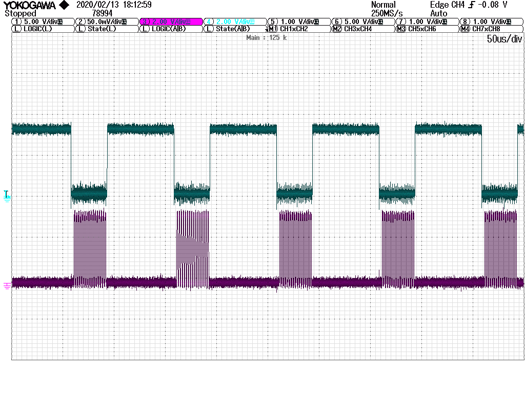
I am using ads7254 external ADC with LaunchPad TMS320F28379D using SPI. I have tried the loopback example and works correctly. but when I load configuration with ADC, I read "0" in "SpiaRegs.SPIRXBUF" register.  The DSP is in master mode, SPI clock is 500KHz. 

I am not receiving anything on SPISOMI, I read 0 always, whenever there is clock. When clock is not present it goes high. Also, there is delay between two SPI channels, which I do not understand why ?

I attach below the SPI configuration.  I have also tried to send to ADC 0x0800 instead of 0x8800, as I want to work in 16-CLK, Dual-SDO Mode (CFR.B11 = 1, CFR.B10 = 0),but I read 0 all the time. 

Thank you. 

#define SPI_BRR        ((200E6 / 4) / 500E3) - 1

            //==============  SPI - A ======================
            //===============================================
            //Init GPIO SPIA
EALLOW ;
            GpioCtrlRegs.GPBPUD.bit.GPIO58 = 0;   // Enable pull-up on GPIO16
            GpioCtrlRegs.GPBPUD.bit.GPIO59 = 0;   // Enable pull-up on GPIO17
            GpioCtrlRegs.GPBPUD.bit.GPIO60 = 0;   // Enable pull-up on GPIO18
            GpioCtrlRegs.GPBPUD.bit.GPIO61 = 0;   // Enable pull-up on GPIO19

            GpioCtrlRegs.GPBQSEL2.bit.GPIO58 = 3;
            GpioCtrlRegs.GPBQSEL2.bit.GPIO59 = 3; // Asynch input GPIO17
            GpioCtrlRegs.GPBQSEL2.bit.GPIO60 = 3; // Asynch input GPIO18
            GpioCtrlRegs.GPBQSEL2.bit.GPIO61 = 3; // Asynch input GPIO19

            GpioCtrlRegs.GPBGMUX2.bit.GPIO58 = 3;   // Configure GPIO16 as SPI
            GpioCtrlRegs.GPBGMUX2.bit.GPIO59 = 3;
            GpioCtrlRegs.GPBGMUX2.bit.GPIO60 = 3;
            GpioCtrlRegs.GPBGMUX2.bit.GPIO61 = 3;

            GpioCtrlRegs.GPBMUX2.bit.GPIO58 = 3;
            GpioCtrlRegs.GPBMUX2.bit.GPIO59 = 3;   // Configure GPIO17 as SPI
            GpioCtrlRegs.GPBMUX2.bit.GPIO60 = 3;   // Configure GPIO18 as SPI
            GpioCtrlRegs.GPBMUX2.bit.GPIO61 = 3;   // Configure GPIO19 as SPI

            GpioCtrlRegs.GPBDIR.bit.GPIO58 = 1;  
            GpioCtrlRegs.GPBDIR.bit.GPIO59 = 0; 
            GpioCtrlRegs.GPBDIR.bit.GPIO60 = 1;   
            GpioCtrlRegs.GPBDIR.bit.GPIO61 = 1;

            //==============  SPI - B ======================
            //==========  Init GPIO SPIB ================


            GpioCtrlRegs.GPAPUD.bit.GPIO24 = 0;   // Enable pull-up on GPIO24
            GpioCtrlRegs.GPAPUD.bit.GPIO25 = 0;   // Enable pull-up on GPIO25
            GpioCtrlRegs.GPAPUD.bit.GPIO26 = 0;   // Enable pull-up on GPIO26
            GpioCtrlRegs.GPAPUD.bit.GPIO27 = 0;   // Enable pull-up on GPIO27

            GpioCtrlRegs.GPAQSEL2.bit.GPIO24 = 3; // Asynch input GPIO24
            GpioCtrlRegs.GPAQSEL2.bit.GPIO25 = 3; // Asynch input GPIO25
            GpioCtrlRegs.GPAQSEL2.bit.GPIO26 = 3; // Asynch input GPIO26
            GpioCtrlRegs.GPAQSEL2.bit.GPIO27 = 3; // Asynch input GPIO27

            GpioCtrlRegs.GPAGMUX2.bit.GPIO24 = 1;   // Configure GPIO24
            GpioCtrlRegs.GPAGMUX2.bit.GPIO25 = 1;
            GpioCtrlRegs.GPAGMUX2.bit.GPIO26 = 1;
            GpioCtrlRegs.GPAGMUX2.bit.GPIO27 = 1;

            GpioCtrlRegs.GPAMUX2.bit.GPIO24 = 2; //as SPI
            GpioCtrlRegs.GPAMUX2.bit.GPIO25 = 2;   // Configure GPIO25 as SPI
            GpioCtrlRegs.GPAMUX2.bit.GPIO26 = 2;   // Configure GPIO26 as SPI
            GpioCtrlRegs.GPAMUX2.bit.GPIO27 = 2;   // Configure GPIO27 as SPI

            GpioCtrlRegs.GPADIR.bit.GPIO24 = 1;
            GpioCtrlRegs.GPADIR.bit.GPIO25 = 0;
            GpioCtrlRegs.GPADIR.bit.GPIO26 = 1;  
            GpioCtrlRegs.GPADIR.bit.GPIO27 = 1;
EDIS; 

void spi_init(){


        //Init SPI A
        SpiaRegs.SPICCR.bit.SPISWRESET=0;  
        SpiaRegs.SPICCR.bit.CLKPOLARITY=0; //Output Rising Edge, Input is latched Falling Edge
        SpiaRegs.SPICCR.bit.HS_MODE =0;    // High Speed Mode DISABLE
        SpiaRegs.SPICCR.bit.SPICHAR=15;
        SpiaRegs.SPICCR.bit.SPILBK=0;      //Loopback Disable (Testing Mode)
        SpiaRegs.SPICTL.bit.MASTER_SLAVE = 1;
        SpiaRegs.SPICTL.bit.TALK = 1;
        SpiaRegs.SPICTL.bit.CLK_PHASE = 0;
        SpiaRegs.SPICTL.bit.SPIINTENA = 0;
        SpiaRegs.SPIBRR.bit.SPI_BIT_RATE=SPI_BRR ;
        SpiaRegs.SPICCR.bit.SPISWRESET=1; 

       //Init SPI B
        SpibRegs.SPICCR.bit.SPISWRESET=0;  
        SpibRegs.SPICCR.bit.CLKPOLARITY=0; //Output Rising Edge, Input is latched Falling Edge
        SpibRegs.SPICCR.bit.HS_MODE =0;    // High Speed Mode DISABLE
        SpibRegs.SPICCR.bit.SPICHAR=15;
        SpibRegs.SPICCR.bit.SPILBK=0;      //Loopback Disable (Testing Mode)
        SpibRegs.SPICTL.bit.MASTER_SLAVE = 1;
        SpibRegs.SPICTL.bit.TALK = 1;
        SpibRegs.SPICTL.bit.CLK_PHASE = 0;
        SpibRegs.SPICTL.bit.SPIINTENA = 0;
        SpibRegs.SPIBRR.bit.SPI_BIT_RATE=SPI_BRR ;
        SpibRegs.SPICCR.bit.SPISWRESET=1; 


}

__interrupt void epwm1_isr(void)
{
         SpiaRegs.SPITXBUF  = 0x8800 ; 
         SpibRegs.SPITXBUF  = 0x8800 ;

        while (! SpiaRegs.SPISTS.bit.INT_FLAG ) {}
         SPI_I_A = SpiaRegs.SPIRXBUF; 
        while (! SpibRegs.SPISTS.bit.INT_FLAG ) {}
         SPI_I_B = SpibRegs.SPIRXBUF;

}

  • Vidhi,

    Based on the inputs provided, I believe you just trying to read ADC results on the falling edge of SPICLK correct?

    Looking into ads7254 DS, it looks like you need to do the following:-

    1) Write CFR = 0x8800 to select 16-CLK,Dual-SDO Mode), this will allow you to select SDO_A outputs ADCA result, SDO_B outputs ADCB result

    - CFR.B15:B12 = 8 corresponds to CFR  write register

    - CFR.B11 = 1 (setting RD_CLK_MODE = 16-CLKmode)

    - CFR.B10 = 0 (Dual-SDOMode selected)

    So, F28379D.SPI needs to be configured as master and transmit 0x8800

    2) Provide dummy transmit.to ADS7254 to have ADS7254 transmit ADC result back to master

    Dummy transfer can initiated by writting 0x000 to SPITXBUF register. After this dummy SPI transfer, you can expect to have ADC result in SPIRXBUF.

    In your code, you are doing to trasmitting 0x8800 twice which actually configure CFR register twice. Try dummy SPI transfer as mentioned above instead.

    I would also encourage you monitor the SPI buses using logic analyzer / oscilloscope.

    Hope this helps.

    Regards,

    Manoj

  • Thank you for the response. 

    yes I am reading ADC value. I am sending 0x8800 to ADC. I am monitoring SPI buses and they seems correct. 

    When I observed SOMI, it is 0 when there is clock as shown in the photo attached. The picture is taken when sent dummy data as you mentioned. but It is the same as when sent 0x8800. 

    I am not  transmitting 0x8800 twice, but I am using 2 channels Spia and Spib. I changed DSP but the same response, Also ADC is working with FPGA, but of course in different mode. 

    I do not understand, what shall I check next.   

  • Hello Vidhi,

    The CFR register value 0x8800 is the correct value for writing to the register with the desired settings mentioned in your first post. However, the ADS7254 defaults to 32-CLK, dual-SDO mode upon power-up. To change the mode, the first command must satisfy the 32-clock minimum requirement as shown in Table 3.

    In your first frame, extend the frame to at least 32 SCLK falling edges by padding the 0x8800 with 0x0000. 

    You also mentioned that DOUT on the ADS7254 goes high when SCLKs are stopped. I would guess that /CS is also going high at this time? When /CS = 1, the interface is disabled and DOUT goes to a high-imepdance tri-state output. Something else sharing the same DOUT line may be pulling this pin high, but I don't believe it is a concern just yet.

    Best regards,

  • Hello sir, 

    Thank you for the reply. I am new to SPI, and hence How can I transfer 32 bit for the first time using FIFO ?

    as SPI can only send 16bit.

  • Hi Vidhi,

    Do you mean that the SPI peripheral can only support 16-bit frames or 16-bit word sizes? I'm not familiar enough with the TMS320F28379D to say what the supported frame lengths are, but I imagine that it's possible to send more than two bytes in a frame (by "frame" I mean the communication between /CS = 0 and /CS = 1). If you find that the SPI peripheral always resets /CS after every 16 bits and you cannot send 32 bits in a single frame, my suggestion would be to control /CS manually with a dedicated GPIO pin that you set high/low as desired. 

    Manoj - can you please confirm whether the SPI frame can be extended beyond 16 bits and explain how to do that for Vidhi?

    Best regards,

  • Hello,

    I changed the GPIO60 to GPIO56 and I read correct value from ADC, but I can read sometimes and most of the time no. So, I decided to do what you suggested Ryan.  

    The clock is of 48 pulses with the following dma configuration. So, I do not think SPI resets after every 16 bits. 

    I meant 1-16 bits at a time. So, I saw the dma example and I have tried following code. but as I have to send first frame 32-bits, I should set as in the code. 

    Now, the doubt is which in which register I should read to see what ADC is sending the master, as "SpiaRegs.SPIRXBUF" is 0. 

    Also, let me know please where I am making mistake. I am receiving something on SOMI, and changing it when I change sensor voltage, But How to confirm that what it is sending is correct or not. 

    //###########################################################################
    //
    // FILE:   Example_2837xDSpi_FFDLB.c
    //
    // TITLE:  SPI Digital Loop Back program.
    //
    //! \addtogroup cpu01_example_list
    //! <h1>SPI Digital Loop Back (spi_loopback)</h1>
    //!
    //!  This program uses the internal loop back test mode of the peripheral.
    //!  Other then boot mode pin configuration, no other hardware configuration
    //!  is required. Interrupts are not used.
    //!
    //!  A stream of data is sent and then compared to the received stream.
    //!  The sent data looks like this: \n
    //!  0000 0001 0002 0003 0004 0005 0006 0007 .... FFFE FFFF \n
    //!  This pattern is repeated forever.
    //!
    //!  \b Watch \b Variables \n
    //!  - \b sdata - sent data
    //!  - \b rdata - received data
    //!
    //
    //###########################################################################
    // $TI Release: F2837xD Support Library v200 $
    // $Release Date: Tue Jun 21 13:00:02 CDT 2016 $
    // $Copyright: Copyright (C) 2013-2016 Texas Instruments Incorporated -
    //             http://www.ti.com/ ALL RIGHTS RESERVED $
    //###########################################################################
    
    //
    // Included Files
    //
    #include "F28x_Project.h"
    
    
    #define BURST         (FIFO_LVL-1)    // burst size should be less than 8
    #define TRANSFER      0              // [(MEM_BUFFER_SIZE/FIFO_LVL)-1]
    #define FIFO_LVL      3               // FIFO Interrupt Level
    
    #pragma DATA_SECTION(sdata, "ramgs0");    // map the TX data to memory
    #pragma DATA_SECTION(rdata, "ramgs1");    // map the RX data to memory
    Uint16 sdata[4];     // Send data buffer
    Uint16 rdata[4];     // Receive data buffer
    Uint16 spi_a[4];
    Uint16 rdata_point;    // Keep track of where we are
                           // in the data stream to check received data
    volatile Uint16 *DMADest;
    volatile Uint16 *DMASource;
    volatile Uint16 done;
    int i=0,mario;
    //
    // Function Prototypes
    //
    __interrupt void local_D_INTCH5_ISR(void);
    __interrupt void local_D_INTCH6_ISR(void);
    void delay_loop(void);
    void dma_init(void);
    void spi_fifo_init(void);
    void error();
    
    void spi_init(void);
    void Init_Pie(void);
    void SPI(void);
    
    
    //Global variables (used to read registers)
    
    float spi_b_1;
    
    int CONT =0;
    
    void main(void){
    
    
    InitSysCtrl();
    InitGpio();
    spi_init();        // init SPI
    Init_Pie();
    
    IER = 0x0000;
    IFR = 0x0000;
    
    
       //Clear all interrupts and initialize PIE vector table:
       //Disable CPU interrupts
       DINT;
    
    
       InitPieCtrl();
    
       //Disable CPU interrupts and clear all CPU interrupt flags:
       IER = 0x0000;
       IFR = 0x0000;
    
    
       InitPieVectTable();
    
        EALLOW;  // This is needed to write to EALLOW protected registers
        PieVectTable.DMA_CH5_INT= &local_D_INTCH5_ISR;
        PieVectTable.DMA_CH6_INT= &local_D_INTCH6_ISR;
        EDIS;   // This is needed to disable write to EALLOW protected registers
    
        dma_init();            // Set up DMA for SPI configuration
        spi_fifo_init();       // Initialize the SPI only
    
        EALLOW;
        CpuSysRegs.SECMSEL.bit.PF2SEL = 1;
        EDIS;
        ERTM;
              PieCtrlRegs.PIECTRL.bit.ENPIE = 1;          // Enable the PIE block
              PieCtrlRegs.PIEIER7.bit.INTx5 = 1;   // Enable PIE Group 7, INT 1 (DMA CH1)
              PieCtrlRegs.PIEIER7.bit.INTx6 = 1;   // Enable PIE Group 7, INT 2 (DMA CH2)
              IER= M_INT7;                         // Enable CPU INT6
              EINT;
    
              // Enable Global Interrupts
              for(i=0; i<4; i++)
                            {
                  sdata[0] = 0x8800;
                  sdata[1] = 0x0000;
                  sdata[2] = 0x8800;
                  sdata[3] = 0x0000;
                                   }
    
              rdata_point = 0;
    
              for(;;)
                {
                 mario++;
    
                 //
                // Initialize the data buffers
                //
                           StartDMACH6();                       // Start SPI RX DMA channel
                           StartDMACH5();                       // Start SPI TX DMA channel
    
                          done = 0;                            // Test is not done yet
    
                           while(!done);                        // wait until the DMA transfer is
                                                                // complete
                           SPI();
                }
    }
    
    //
    // delay_loop - Function to add delay
    //
    void delay_loop()
    {
        long i;
        for (i = 0; i < 1000000; i++) {}
    }
    
    //
    // error - Halt debugger when error received
    //
    void error(void)
    {
       asm("     ESTOP0");  //Test failed!! Stop!
       for (;;);
    }
    
    //
    // spi_fifo_init - Initialize SPIB FIFO
    //
    void spi_fifo_init()
    {
        //
        // Initialize SPI FIFO registers
        //
        SpiaRegs.SPIFFRX.all=0x2040;             // RX FIFO enabled, clear FIFO int
        SpiaRegs.SPIFFRX.bit.RXFFIL = FIFO_LVL;  // Set RX FIFO level
    
        SpiaRegs.SPIFFTX.all=0xE040;             // FIFOs enabled, TX FIFO released,
        SpiaRegs.SPIFFTX.bit.TXFFIL = FIFO_LVL;  // Set TX FIFO level
    
        //
        // Initialize core SPI registers
        //
        spi_init();
    }
    
    //
    // dma_init - DMA setup for both TX and RX channels.
    //
    void dma_init()
    {
        //
        // Initialize DMA
        //
        DMAInitialize();
    
        DMASource = (volatile Uint16 *)sdata;
        DMADest = (volatile Uint16 *)rdata;
    
        //
        // configure DMACH5 for TX
        //
        DMACH5AddrConfig(&SpiaRegs.SPITXBUF,DMASource);
        DMACH5BurstConfig(BURST,1,0);         // Burst size, src step, dest step
        DMACH5TransferConfig(TRANSFER,1,0);   // transfer size, src step, dest step
        DMACH5ModeConfig(DMA_SPIATX,PERINT_ENABLE,ONESHOT_DISABLE,CONT_DISABLE,
                         SYNC_DISABLE,SYNC_SRC,OVRFLOW_DISABLE,SIXTEEN_BIT,
                         CHINT_END,CHINT_ENABLE);
    
        //
        // configure DMA CH2 for RX
        //
        DMACH6AddrConfig(DMADest,&SpiaRegs.SPIRXBUF);
        DMACH6BurstConfig(BURST,0,1);
        DMACH6TransferConfig(TRANSFER,0,1);
        DMACH6ModeConfig(DMA_SPIARX,PERINT_ENABLE,ONESHOT_DISABLE,CONT_DISABLE,
                         SYNC_DISABLE,SYNC_SRC,OVRFLOW_DISABLE,SIXTEEN_BIT,
                         CHINT_END,CHINT_ENABLE);
    }
    
    //
    // local_D_INTCH5_ISR - DMA Channel 5 ISR
    //
    __interrupt void local_D_INTCH5_ISR(void)
    {
        EALLOW;  // NEED TO EXECUTE EALLOW INSIDE ISR !!!
        DmaRegs.CH5.CONTROL.bit.HALT=1;
        PieCtrlRegs.PIEACK.all = PIEACK_GROUP7; // ACK to receive more interrupts
                                                // from this PIE group
        EDIS;
        return;
    }
    
    //
    // local_D_INTCH6_ISR - DMA Channel 6 ISR
    //
    __interrupt void local_D_INTCH6_ISR(void)
    {
    
        Uint16 i;
    
        EALLOW;  // NEED TO EXECUTE EALLOW INSIDE ISR !!!
        DmaRegs.CH6.CONTROL.bit.HALT = 1;
        PieCtrlRegs.PIEACK.all = PIEACK_GROUP7; // ACK to receive more interrupts
                                                // from this PIE group
        EDIS;
    
        for( i = 0; i<4; i++ )
        {
            //
            // check for data integrity
            //
           /* if(rdata[i] != i)
            {
                error();
            }*/
            spi_a[i] = rdata[i];
        }
    
        done = 1;  // test done.
        return;
    }
    void spi_init(){
    
        EALLOW;
            //==============  SPI - B ======================
            //===============================================
            //Init GPIO SPIB
    
            GpioCtrlRegs.GPBPUD.bit.GPIO56 = 1;   // Disable pull-up on GPIO22
            GpioCtrlRegs.GPBQSEL2.bit.GPIO56 = 3; //
            GpioCtrlRegs.GPBGMUX2.bit.GPIO56=0;// Configure GPIO22
            GpioCtrlRegs.GPBMUX2.bit.GPIO56=1;
            GpioCtrlRegs.GPBDIR.bit.GPIO56=1;    //
    
            GpioCtrlRegs.GPBPUD.bit.GPIO58 = 1;   // DIsable pull-up on GPIO23
            GpioCtrlRegs.GPBQSEL2.bit.GPIO58 = 3; // Asynch input GPIO23
            GpioCtrlRegs.GPBGMUX2.bit.GPIO58=3;
            GpioCtrlRegs.GPBMUX2.bit.GPIO58=3;   // Configure GPIO23
            GpioCtrlRegs.GPBDIR.bit.GPIO58=1;
    
            GpioCtrlRegs.GPBPUD.bit.GPIO59 = 1;   // Disable pull-up on GPIO24
            GpioCtrlRegs.GPBQSEL2.bit.GPIO59 = 3; // Asynch input GPIO24
            GpioCtrlRegs.GPBGMUX2.bit.GPIO59 =3;
            GpioCtrlRegs.GPBMUX2.bit.GPIO59 =3;   // Configure GPIO24
            GpioCtrlRegs.GPBDIR.bit.GPIO59 =0;
    
            GpioCtrlRegs.GPBPUD.bit.GPIO61  = 0;   // Disable pull-up on GPIO25
            GpioCtrlRegs.GPBQSEL2.bit.GPIO61 = 3; // Asynch input GPIO25
            GpioCtrlRegs.GPBGMUX2.bit.GPIO61=3;
            GpioCtrlRegs.GPBMUX2.bit.GPIO61=3;   // Configure GPIO25
            GpioCtrlRegs.GPBDIR.bit.GPIO61=1;
       //     0: Configures pin as input.
        //    1: Configures pin as output.


            // Initialize SPI-A
    
            // Set reset low before configuration changes
            // Clock polarity (0 == rising, 1 == falling)
            // 16-bit character
            // Enable loop-back
            SpiaRegs.SPICCR.bit.SPISWRESET = 0;
            SpiaRegs.SPICCR.bit.CLKPOLARITY = 0;
            SpiaRegs.SPICCR.bit.SPICHAR = (16-1);
            SpiaRegs.SPICCR.bit.SPILBK = 1;
    
            // Enable master (0 == slave, 1 == master)
            // Enable transmission (Talk)
            // Clock phase (0 == normal, 1 == delayed)
            // SPI interrupts are disabled
            SpiaRegs.SPICTL.bit.MASTER_SLAVE = 1;
            SpiaRegs.SPICTL.bit.TALK = 1;
            SpiaRegs.SPICTL.bit.CLK_PHASE = 0;
            SpiaRegs.SPICTL.bit.SPIINTENA = 0;
    
            // Set the baud rate
            SpiaRegs.SPIBRR.bit.SPI_BIT_RATE = SPI_BRR;
    
            // Set FREE bit
            // Halting on a breakpoint will not halt the SPI
            SpiaRegs.SPIPRI.bit.FREE = 1;
    
            // Release the SPI from reset
            SpiaRegs.SPICCR.bit.SPISWRESET = 1;
    
            EDIS;
    
    }


    void Init_Pie(void)
    {
           DINT;
    
           // Disable the PIE
           PieCtrlRegs.PIECTRL.bit.ENPIE = 0;
    
           // Clear all PIEIER registers:
           PieCtrlRegs.PIEIER1.all = 0;
    
           PieCtrlRegs.PIEIFR1.all = 0;
    
    }


    void SPI(void){
    
      //  while(! SpiaRegs.SPIFFRX.bit.RXFFST) { }
      //  spi_b_1= SpiaRegs.SPIRXBUF;
     /*   if (CONT==1){
    
             SpiaRegs.SPITXBUF=0x8800;
             while ( ! SpiaRegs.SPISTS.bit.INT_FLAG ) {}
                     spi_b_1= SpiaRegs.SPIRXBUF;
    
    
             }
    
            if (CONT>1){
                SpiaRegs.SPITXBUF=0x0000;
                      while ( ! SpiaRegs.SPISTS.bit.INT_FLAG ) {}
                              spi_b_1= SpiaRegs.SPIRXBUF;
    
             }
    */
    
    }


  • Vidhi,

    Below thread explains how to transmit 32 bits at a time. When are trying to read the SPI data received from ADC. You need to wait for

    RXFFINT flag to be set and then read the SPIRXBUF register can be used to read the results stored in FIFO

    Regards,

    Manoj