Hi,
my customer met a strange phenomenon.
Their code is:
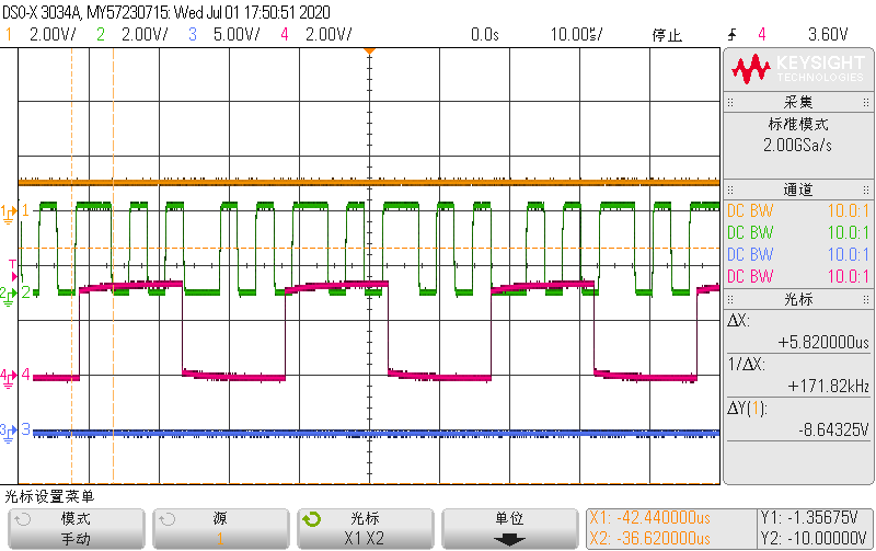
generate SOCA with EPWM4 count to 0 or PRD, every SOCA will trigger ADC conversion from SOC0-SOC15.
They also generate PWMISR at EPWM4 count to 0 or PRD, ISR happens every 15us.
In PWMISR, we will read ADCRESULT15 corresponding to SOC15.
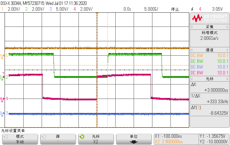
We find that the result will only reflect the actual signal value 2 ISRs later, which is 30us.
Let's say at T=0us SOCA is triggered, at some time SOC15 start to convert. If all 16 SOCs can be converted within 15us, we should be able to read the correct result at PWMISR generated at T=15us. But now we are not able to do that, we have to wait another 15us to read the correct result in the next PWMISR.
For SOC1, we can read the correct result at PWMISR generated to T=15us.
The ADC setting code is as below:
// Checkin $Date: December 16, 2009   16:43:59 $
//###########################################################################
//
// FILE:    DSP2802x_Adc.c
//
// TITLE:   DSP2802x ADC Initialization & Support Functions.
//
//###########################################################################
// $TI Release: 2802x C/C++ Header Files V1.26 $
// $Release Date: February 2, 2010 $
//###########################################################################
//--------------------------------------------------------
// Product: Three Phase Vienna PFC
// Running on TMS320F2802x
// External clock is 20MHz, PLL * 4/2 , CPU-Clock 40 MHz
// Date: from 2011-10-9  , (Copyright) lvyougen
// Version:1.00
//--------------------------------------------------------

#include "DSP28x_Project.h"     // Headerfile Include File

#define ADC_usDELAY  1000L

//---------------------------------------------------------------------------
// InitAdc:
//---------------------------------------------------------------------------
// This function initializes ADC to a known state.
//
// NOTE: ADC INIT IS DIFFERENT ON 2802x DEVICES COMPARED TO OTHER 28X DEVICES
//
void InitAdc(void)
{
    extern void DSP28x_usDelay(Uint32 Count);

    // *IMPORTANT*
    // The Device_cal function, which copies the ADC calibration values from TI reserved
    // OTP into the ADCREFSEL and ADCOFFTRIM registers, occurs automatically in the
    // Boot ROM. If the boot ROM code is bypassed during the debug process, the
    // following function MUST be called for the ADC to function according
    // to specification. The clocks to the ADC MUST be enabled before calling this
    // function.
    // See the device data manual and/or the ADC Reference
    // Manual for more information.

        EALLOW;
        SysCtrlRegs.PCLKCR0.bit.ADCENCLK = 1;
        (*Device_cal)();
        EDIS;

    // To powerup the ADC the ADCENCLK bit should be set first to enable
    // clocks, followed by powering up the bandgap, reference circuitry, and ADC core.
    // Before the first conversion is performed a 5ms delay must be observed
    // after power up to give all analog circuits time to power up and settle

    // Please note that for the delay function below to operate correctly the
    // CPU_RATE define statement in the DSP2802x_Examples.h file must
    // contain the correct CPU clock period in nanoseconds.
    EALLOW;
    AdcRegs.ADCCTL1.bit.ADCBGPWD  = 1;      // Power ADC BG
    AdcRegs.ADCCTL1.bit.ADCREFPWD = 1;      // Power reference
    AdcRegs.ADCCTL1.bit.ADCPWDN   = 1;      // Power ADC
    AdcRegs.ADCCTL1.bit.ADCENABLE = 1;      // Enable ADC
    AdcRegs.ADCCTL1.bit.ADCREFSEL = 1;      // External VREFHI/VREFLO pins used for reference generation.

	AdcRegs.ADCCTL1.bit.TEMPCONV  = 1; //Connect channel A5 internally to the temperature sensor
	//AdcRegs.ADCCTL2
    EDIS;

    DELAY_US(ADC_usDELAY);         // Delay before converting ADC channels

	AdcOffsetSelfCal();

	EALLOW;

	AdcRegs.ADCSOC0CTL.bit.CHSEL= 0x01;	//va,// SOCx Channel Select: ADCINA1
    AdcRegs.ADCSOC1CTL.bit.CHSEL= 0x02;	//vb
    AdcRegs.ADCSOC2CTL.bit.CHSEL= 0x03;	//vc
    AdcRegs.ADCSOC3CTL.bit.CHSEL= 0x04;	//ia1->ia
    AdcRegs.ADCSOC4CTL.bit.CHSEL= 0x07;	//ia2->ib, 6->7
    AdcRegs.ADCSOC5CTL.bit.CHSEL= 0x0A;	//ib1->ic, 7->A
    AdcRegs.ADCSOC6CTL.bit.CHSEL= 0x06;	//ib2->Fan1Bad, 9->6
    AdcRegs.ADCSOC7CTL.bit.CHSEL= 0x09;	//ic1->Fan2bad, A->9
    AdcRegs.ADCSOC8CTL.bit.CHSEL= 0x0B;	//ic2->Fan3bad
    AdcRegs.ADCSOC9CTL.bit.CHSEL= 0x0C;	//vp
    AdcRegs.ADCSOC10CTL.bit.CHSEL= 0x0E;//vn
    AdcRegs.ADCSOC11CTL.bit.CHSEL= 0x0F;	//vp_ovp, A5
    AdcRegs.ADCSOC12CTL.bit.CHSEL= 0x0F;	//vn_ovp, A6
    AdcRegs.ADCSOC13CTL.bit.CHSEL= 0x0F;	//Temp_Amb, A2
    AdcRegs.ADCSOC14CTL.bit.CHSEL= 0x0F;	//Temp_pfc, A3
    AdcRegs.ADCSOC15CTL.bit.CHSEL= 0x0F;	//Temp_DcdcMos_A4, Vcc_Fan_A0, VfanBad_A1, Vref3V_A7
											// and select to ADCINA5 for internal the temperature sensor

	AdcRegs.ADCSOC0CTL.bit.ACQPS  = 6;	// SOCx Acquisition Prescale: Sample window is 7 cycles long (6 + 1 clock cycles).
    AdcRegs.ADCSOC1CTL.bit.ACQPS  = 6;
    AdcRegs.ADCSOC2CTL.bit.ACQPS  = 6;
    AdcRegs.ADCSOC3CTL.bit.ACQPS  = 6;
    AdcRegs.ADCSOC4CTL.bit.ACQPS  = 6;
    AdcRegs.ADCSOC5CTL.bit.ACQPS  = 6;
    AdcRegs.ADCSOC6CTL.bit.ACQPS  = 6;
    AdcRegs.ADCSOC7CTL.bit.ACQPS  = 6;
    AdcRegs.ADCSOC8CTL.bit.ACQPS  = 6;
    AdcRegs.ADCSOC9CTL.bit.ACQPS  = 6;
    AdcRegs.ADCSOC10CTL.bit.ACQPS = 6;
    AdcRegs.ADCSOC11CTL.bit.ACQPS = 6;
    AdcRegs.ADCSOC12CTL.bit.ACQPS = 6;
    AdcRegs.ADCSOC13CTL.bit.ACQPS = 6;
    AdcRegs.ADCSOC14CTL.bit.ACQPS = 6;
    AdcRegs.ADCSOC15CTL.bit.ACQPS = 6;

	AdcRegs.ADCSOC0CTL.bit.TRIGSEL = 0x0B;	// SOCx Trigger Source Select: ADCTRIG9 – ePWM3, ADCSOCA
	AdcRegs.ADCSOC1CTL.bit.TRIGSEL = 0x0B;
	AdcRegs.ADCSOC2CTL.bit.TRIGSEL = 0x0B;
	AdcRegs.ADCSOC3CTL.bit.TRIGSEL = 0x0B;
	AdcRegs.ADCSOC4CTL.bit.TRIGSEL = 0x0B;
	AdcRegs.ADCSOC5CTL.bit.TRIGSEL = 0x0B;
	AdcRegs.ADCSOC6CTL.bit.TRIGSEL = 0x0B;
	AdcRegs.ADCSOC7CTL.bit.TRIGSEL = 0x0B;
	AdcRegs.ADCSOC8CTL.bit.TRIGSEL = 0x0B;
	AdcRegs.ADCSOC9CTL.bit.TRIGSEL = 0x0B;
	AdcRegs.ADCSOC10CTL.bit.TRIGSEL = 0x0B;
	AdcRegs.ADCSOC11CTL.bit.TRIGSEL = 0x0B;
	AdcRegs.ADCSOC12CTL.bit.TRIGSEL = 0x0B;
	AdcRegs.ADCSOC13CTL.bit.TRIGSEL = 0x0B;
	AdcRegs.ADCSOC14CTL.bit.TRIGSEL = 0x0B;
	AdcRegs.ADCSOC15CTL.bit.TRIGSEL = 0x0B;

	StartSOC();	//enables SOCA pulse

	EDIS;
}

void InitAdcAio()
{

   EALLOW;

/* Configure ADC pins using AIO regs*/
// This specifies which of the possible AIO pins will be Analog input pins.
// NOTE: AIO1,3,5,7-9,11,13,15 are analog inputs in all AIOMUX1 configurations.
// Comment out other unwanted lines.

    GpioCtrlRegs.AIOMUX1.bit.AIO2 = 2;    // Configure AIO2 for A2 (analog input) operation
    GpioCtrlRegs.AIOMUX1.bit.AIO4 = 2;    // Configure AIO4 for A4 (analog input) operation
    GpioCtrlRegs.AIOMUX1.bit.AIO6 = 2;    // Configure AIO6 for A6 (analog input) operation
    GpioCtrlRegs.AIOMUX1.bit.AIO10 = 2;   // Configure AIO10 for B2 (analog input) operation
    GpioCtrlRegs.AIOMUX1.bit.AIO12 = 2;   // Configure AIO12 for B4 (analog input) operation
    GpioCtrlRegs.AIOMUX1.bit.AIO14 = 2;   // Configure AIO14 for B6 (analog input) operation

    EDIS;
}

/* AdcoffsetSelfCal-
   This function re-calibrates the ADC zero offset error by converting the VREFLO reference with
   the ADC and modifying the ADCOFFTRIM register. VREFLO is sampled by the ADC using an internal
   MUX select which connects VREFLO to A5 without sacrificing an external ADC pin. This
   function calls two other functions:
   - AdcChanSelect(channel) ?selects the ADC channel to convert
   - AdcConversion() ?initiates several ADC conversions and returns the average
*/
void AdcOffsetSelfCal()
{
    Uint16 AdcConvMean;
    EALLOW;
    AdcRegs.ADCCTL1.bit.ADCREFSEL = 1;                  //External VREFHI/VREFLO pins used for reference generation.
    AdcRegs.ADCCTL1.bit.VREFLOCONV = 1;                 //Select VREFLO internal connection on B5
    AdcChanSelect(13);                                  //Select channel B5 for all SOC
    AdcRegs.ADCOFFTRIM.bit.OFFTRIM = 80;                //Apply artificial offset (+80) to account for a negative offset that may reside in the ADC core
    AdcConvMean = AdcConversion();                      //Capture ADC conversion on VREFLO
    AdcRegs.ADCOFFTRIM.bit.OFFTRIM = 80 - AdcConvMean;  //Set offtrim register with new value (i.e remove artical offset (+80) and create a two's compliment of the offset error)
    AdcRegs.ADCCTL1.bit.VREFLOCONV = 0;                 //Select external ADCIN5 input pin on B5
    EDIS;
}

/*  AdcChanSelect-
    This function selects the ADC channel to convert by setting all SOC channel selects to a single channel.

     * IMPORTANT * This function will overwrite previous SOC channel select settings. Recommend saving
           the previous settings.
 */
void AdcChanSelect(Uint16 ch_no)
{
    AdcRegs.ADCSOC0CTL.bit.CHSEL= ch_no;
    AdcRegs.ADCSOC1CTL.bit.CHSEL= ch_no;
    AdcRegs.ADCSOC2CTL.bit.CHSEL= ch_no;
    AdcRegs.ADCSOC3CTL.bit.CHSEL= ch_no;
    AdcRegs.ADCSOC4CTL.bit.CHSEL= ch_no;
    AdcRegs.ADCSOC5CTL.bit.CHSEL= ch_no;
    AdcRegs.ADCSOC6CTL.bit.CHSEL= ch_no;
    AdcRegs.ADCSOC7CTL.bit.CHSEL= ch_no;
    AdcRegs.ADCSOC8CTL.bit.CHSEL= ch_no;
    AdcRegs.ADCSOC9CTL.bit.CHSEL= ch_no;
    AdcRegs.ADCSOC10CTL.bit.CHSEL= ch_no;
    AdcRegs.ADCSOC11CTL.bit.CHSEL= ch_no;
    AdcRegs.ADCSOC12CTL.bit.CHSEL= ch_no;
    AdcRegs.ADCSOC13CTL.bit.CHSEL= ch_no;
    AdcRegs.ADCSOC14CTL.bit.CHSEL= ch_no;
    AdcRegs.ADCSOC15CTL.bit.CHSEL= ch_no;
} //end AdcChanSelect

/* AdcConversion -
   This function initiates several ADC conversions and returns the average. It uses ADCINT1 and ADCINT2
   to "ping-pong" between SOC0-7 and SOC8-15 and is referred to as "ping-pong" sampling.

     * IMPORTANT * This function will overwrite previous ADC settings. Recommend saving previous settings.
*/
Uint16 AdcConversion(void)
{
    Uint16 index, SampleSize, Mean, ACQPS_Value;
    Uint32 Sum;

    index       = 0;            //initialize index to 0
    SampleSize  = 256;          //set sample size to 256 (**NOTE: Sample size must be multiples of 2^x where is an integer >= 4)
    Sum         = 0;            //set sum to 0
    Mean        = 999;          //initialize mean to known value

    //Set the ADC sample window to the desired value (Sample window = ACQPS + 1)
    ACQPS_Value = 6;
    AdcRegs.ADCSOC0CTL.bit.ACQPS  = ACQPS_Value;
    AdcRegs.ADCSOC1CTL.bit.ACQPS  = ACQPS_Value;
    AdcRegs.ADCSOC2CTL.bit.ACQPS  = ACQPS_Value;
    AdcRegs.ADCSOC3CTL.bit.ACQPS  = ACQPS_Value;
    AdcRegs.ADCSOC4CTL.bit.ACQPS  = ACQPS_Value;
    AdcRegs.ADCSOC5CTL.bit.ACQPS  = ACQPS_Value;
    AdcRegs.ADCSOC6CTL.bit.ACQPS  = ACQPS_Value;
    AdcRegs.ADCSOC7CTL.bit.ACQPS  = ACQPS_Value;
    AdcRegs.ADCSOC8CTL.bit.ACQPS  = ACQPS_Value;
    AdcRegs.ADCSOC9CTL.bit.ACQPS  = ACQPS_Value;
    AdcRegs.ADCSOC10CTL.bit.ACQPS = ACQPS_Value;
    AdcRegs.ADCSOC11CTL.bit.ACQPS = ACQPS_Value;
    AdcRegs.ADCSOC12CTL.bit.ACQPS = ACQPS_Value;
    AdcRegs.ADCSOC13CTL.bit.ACQPS = ACQPS_Value;
    AdcRegs.ADCSOC14CTL.bit.ACQPS = ACQPS_Value;
    AdcRegs.ADCSOC15CTL.bit.ACQPS = ACQPS_Value;


    //Enable ping-pong sampling

    // Enabled ADCINT1 and ADCINT2
    AdcRegs.INTSEL1N2.bit.INT1E = 1;
    AdcRegs.INTSEL1N2.bit.INT2E = 1;

    // Disable continuous sampling for ADCINT1 and ADCINT2
    AdcRegs.INTSEL1N2.bit.INT1CONT = 0;
    AdcRegs.INTSEL1N2.bit.INT2CONT = 0;

    AdcRegs.ADCCTL1.bit.INTPULSEPOS = 1;    //ADCINTs trigger at end of conversion

    // Setup ADCINT1 and ADCINT2 trigger source
    AdcRegs.INTSEL1N2.bit.INT1SEL = 6;      //EOC6 triggers ADCINT1
    AdcRegs.INTSEL1N2.bit.INT2SEL = 14;     //EOC14 triggers ADCINT2

    // Setup each SOC's ADCINT trigger source
    AdcRegs.ADCINTSOCSEL1.bit.SOC0  = 2;    //ADCINT2 starts SOC0-7
    AdcRegs.ADCINTSOCSEL1.bit.SOC1  = 2;
    AdcRegs.ADCINTSOCSEL1.bit.SOC2  = 2;
    AdcRegs.ADCINTSOCSEL1.bit.SOC3  = 2;
    AdcRegs.ADCINTSOCSEL1.bit.SOC4  = 2;
    AdcRegs.ADCINTSOCSEL1.bit.SOC5  = 2;
    AdcRegs.ADCINTSOCSEL1.bit.SOC6  = 2;
    AdcRegs.ADCINTSOCSEL1.bit.SOC7  = 2;
    AdcRegs.ADCINTSOCSEL2.bit.SOC8  = 1;    //ADCINT1 starts SOC8-15
    AdcRegs.ADCINTSOCSEL2.bit.SOC9  = 1;
    AdcRegs.ADCINTSOCSEL2.bit.SOC10 = 1;
    AdcRegs.ADCINTSOCSEL2.bit.SOC11 = 1;
    AdcRegs.ADCINTSOCSEL2.bit.SOC12 = 1;
    AdcRegs.ADCINTSOCSEL2.bit.SOC13 = 1;
    AdcRegs.ADCINTSOCSEL2.bit.SOC14 = 1;
    AdcRegs.ADCINTSOCSEL2.bit.SOC15 = 1;

    DELAY_US(ADC_usDELAY);                  // Delay before converting ADC channels


    //ADC Conversion

    AdcRegs.ADCSOCFRC1.all = 0x00FF;  // Force Start SOC0-7 to begin ping-pong sampling

    while( index < SampleSize ){

        //Wait for ADCINT1 to trigger, then add ADCRESULT0-7 registers to sum
        while (AdcRegs.ADCINTFLG.bit.ADCINT1 == 0){}
        AdcRegs.ADCINTFLGCLR.bit.ADCINT1 = 1;   //Must clear ADCINT1 flag since INT1CONT = 0
        Sum += AdcResult.ADCRESULT0;
        Sum += AdcResult.ADCRESULT1;
        Sum += AdcResult.ADCRESULT2;
        Sum += AdcResult.ADCRESULT3;
        Sum += AdcResult.ADCRESULT4;
        Sum += AdcResult.ADCRESULT5;
        Sum += AdcResult.ADCRESULT6;
        Sum += AdcResult.ADCRESULT7;

        //Wait for ADCINT2 to trigger, then add ADCRESULT8-15 registers to sum
        while (AdcRegs.ADCINTFLG.bit.ADCINT2 == 0){}
        AdcRegs.ADCINTFLGCLR.bit.ADCINT2 = 1;   //Must clear ADCINT2 flag since INT2CONT = 0
        Sum += AdcResult.ADCRESULT8;
        Sum += AdcResult.ADCRESULT9;
        Sum += AdcResult.ADCRESULT10;
        Sum += AdcResult.ADCRESULT11;
        Sum += AdcResult.ADCRESULT12;
        Sum += AdcResult.ADCRESULT13;
        Sum += AdcResult.ADCRESULT14;
        Sum += AdcResult.ADCRESULT15;

        index+=16;

    } // end data collection

    //Disable ADCINT1 and ADCINT2 to STOP the ping-pong sampling
    AdcRegs.INTSEL1N2.bit.INT1E = 0;
    AdcRegs.INTSEL1N2.bit.INT2E = 0;

    Mean = Sum / SampleSize;    //Calculate average ADC sample value

    return Mean;                //return the average

}//end AdcConversion

//===========================================================================
// End of file.
//===========================================================================