This thread has been locked.

If you have a related question, please click the "Ask a related question" button in the top right corner. The newly created question will be automatically linked to this question.

TMS320F2812: 使用TMS320F2812PGFA 的部分产品误报警 False alarms for some products using TMS320F2812PGFA

Part Number: TMS320F2812

Hi,

我司生产一款电流检测仪器,用到的是TMS320F2812PGFA 芯片。

Our company produces a current detection instrument, which uses the TMS320F2812PGFA chip.

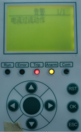
在使用过程中发现某些TMS320F2812PGFA 芯片会导致仪器检测电流误报警,并且按复位键不能复位。同一块电路板,换另外一块TMS320F2812PGFA 芯片后就恢复正常了。查规格书:The F281x ADC has a maximum offset error of ± 80 LSB and a maximum gain error of ± 200 LSB. Themaximum values for both gain and offset error for F280x/F280xx parts are ± 60 LSB.

During use, it is found that some TMS320F2812PGFA chips will cause the instrument to detect the current false alarm, and the reset button cannot be reset. The same circuit board, replaced by another TMS320F2812PGFA chip, returned to normal. Check specifications:The F281x ADC has a maximum offset error of ± 80 LSB and a maximum gain error of ± 200 LSB. Themaximum values for both gain and offset error for F280x/F280xx parts are ± 60 LSB.
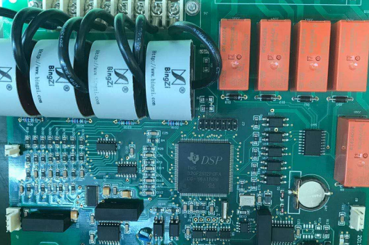
初步怀疑是ADC的误差导致。我应该如何验证TMS320F2812PGFA 的ADC的各项误差范围都是在TMS320F2812PGFA 规格范围内呢?
The preliminary suspicion is that the ADC error is caused. How should I verify that the various error ranges of the TMS320F2812PGFA ADC are within the TMS320F2812PGFA specifications?
期待您的解答,谢谢!
Looking forward to your answer, thank you!
  • Tao,

    You are correct that as a max/min TI expects the device to fall within that spec over the full operating range of the device.  While there will be some device to device variance, they should all meet the specification.

    One note I will make on the gain error is that there is a temperature coefficient associated with the internal reference(which is the major contributor of the gain error) so if you have a large temperature gradient you will see movement.

    With that said, if you can provide me with the voltage range you will give to the ADC I will reply back with some error formulas to help explain the max error you could see and we can go from there.

    In terms of a test in real time, do you have a fixed voltage reference, or for debug an unused ADC channel on the F281x?  If so we could sample this known voltage and see the error term on that device.  So long as we know the ideal conversion we can calculate the error.

    Best,
    Matthew

  • Hi,

    常温25℃下测试,基准电压是3V,测试电流是5A,设计是超过0.3A则会报警。最大误差计算是否这样:200LSB(14.64mV)(14.64mV/3V)*5A=0.0244A测试结果看,已经超出了IC最大误差范围了。此设计用到8ADC脚,未用到的ADCIN脚已短接到地。如果没有电流传感器,测试ADC也超过了误差的最大值。信号地与模拟地有用磁珠做隔离。

    Test at room temperature of 25°C, the reference voltage is 3V, the test current is 5A, and the design is over 0.3A, it will alarm. Is the maximum error calculation like this: 200LSB (14.64mV), (14.64mV/3V)*5A=0.0244A. From the test results, it has exceeded the maximum error range of the IC. This design uses 8 ADC pins, and the unused ADCIN pin has been shorted to ground. If there is no current sensor, the test ADC also exceeds the maximum error.The signal ground and the analog ground are isolated by magnetic beads.

    我有以下两个问题:

    I have the following two questions:

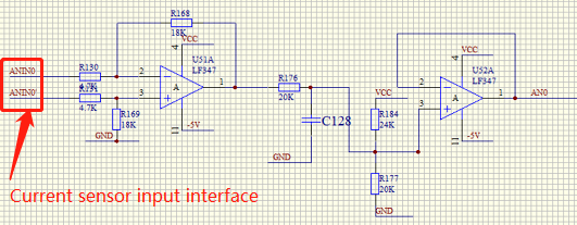
    1,如果没有电流传感器,需要将传感器的两个输入接口短接或直接接地来测试吗?

    1. If there is no current sensor, do I need to short-circuit or directly ground the two input interfaces of the sensor for testing?

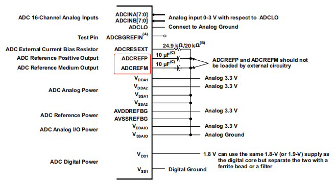
    2,目前检测到客户原理图有点问题,如图,ADCREFPADCREFM悬空,没有接电容到地。这种情况会导致个别IC输出误差很大吗

    1. At present, it is detected that there is a problem with the customer's schematic diagram. ADCREFP and ADCREFM are floating, and the capacitor is not connected to the ground. Will this situation cause large errors in individual IC output?

  • Tao,

    I want to address the comment on ADCREFP/REFM first.  These connections are required for the proper performance of the ADC, as they buffer the internally generated reference voltages.  The caps must be connected to VSSA and NOT floating.  This is likely causing noise and poor/out of spec performance of the converter.

    For the unused current sensor, my concern is that if this would drive the output of the amplifier to the voltage rail.  There is 18kOhm PD on the non inverting input in this case(but also a path to ground for a gain), but customer may want to simulate the effect of a float on the inverting in this case.  Keep in mind that the C2000 is a 3.3V device, and the ADC is unipolar; i.e. 0V/VSSA is the min allowed input voltage.

    If the rails of the op-amps are <0V(the schematic is showing -5V) or >3.3V then it may be possible a floating input would resolve to an op-amp rail, which would damage the C2000 if over/under voltage.

    Best,

    Matthew

  • Dear  Matthew,

    Thanks for the technical support, I will continue to verify, thank you!

    Best,

    Tao