This thread has been locked.

If you have a related question, please click the "Ask a related question" button in the top right corner. The newly created question will be automatically linked to this question.

CCS/TMS320F28377D: In 28377, does there exist the concept of clock for the CLB module ?

Part Number: TMS320F28377D
Other Parts Discussed in Thread: C2000WARE

Tool/software: Code Composer Studio

Hello, I'm trying to use CLB module to protect the PWM signals. The whole procedure is shown as the following picture and is similar to the demo "clb_ex4_pwm_protection".

My intention is:

GPIO2,3 is set to generate the EPWM2 signals.  GPIO16 is connected to a button. When the button is pressed, the I/O will be low level.

Therefore, GPIO16 is utilized to stimulate the error signal.

In normal situation, GPIO2,3 can generate the complentary PWM signals. When the button is pressed, the output of GPIO2,3 should be low level. 

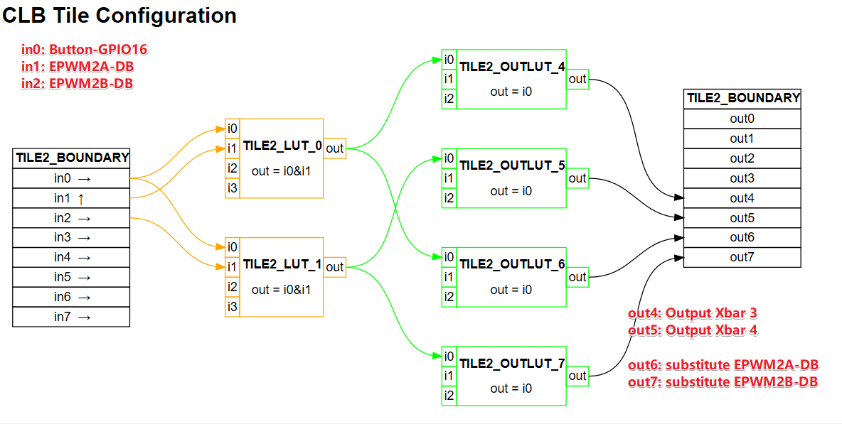
Tile2  functions as an And Gate.

I followed the instructions of the user's guide and the answers presented on the forum. However, I still come across the problem: 

GPIO2,3 can generate the PWM signals, but the GPIO14,15 can't.  It seems that the CLB module does not work.

Some detailed explanation is included in the code.

My code is :

void main(void)
{

    InitSysCtrl();  // system initial 200MHz

    InitGpio();

    InitEPwm1Gpio();   // GPIO0,1 is connected with two LED, and denotes the state of button
    InitEPwm2Gpio();    // EPWM2A,B is the generated PWM signals.

    //GPIO16 is set as I/O and is connected to a button.
    //When the button is pressed, the low level denotes the PWM faults
    //and the PWM signals should be blocked.
    GPIO_SetupPinMux(16,0,0);
    GPIO_SetupPinOptions(16, 0, GPIO_PULLUP);  //


    DINT;

    InitPieCtrl();

    IER = 0x0000;
    IFR = 0x0000;

    InitPieVectTable();


    EALLOW;
    CpuSysRegs.PCLKCR0.bit.TBCLKSYNC =0;
    EDIS;

    InitEPwm2Example();  // 10kHz

    EALLOW;
    CpuSysRegs.PCLKCR0.bit.TBCLKSYNC =1;
    EDIS;

    IER = 0;  // interrupt is disabled


// ------- The code above can work normally. My question is about the setting of CLB Regs.
EALLOW; // Set GPIO16 as Input Xbar1 XBAR_setInputPin(XBAR_INPUT1, 16); //Set InputXbar 1 as XBAR_AUXSIG0 HWREG(XBAR_CLB_CFG_REG_BASE + XBAR_O_AUXSIG0MUX0TO15CFG) |= 4; // Enable XBAR_AUXSIG0 HWREG(XBAR_CLB_EN_REG_BASE + XBAR_AUXSIG0) |= XBAR_MUX01; EDIS; // choose CLB2_BASE CLB_configLocalInputMux(CLB2_BASE, CLB_IN0, CLB_LOCAL_IN_MUX_GLOBAL_IN); CLB_configLocalInputMux(CLB2_BASE, CLB_IN1, CLB_LOCAL_IN_MUX_GLOBAL_IN); CLB_configLocalInputMux(CLB2_BASE, CLB_IN2, CLB_LOCAL_IN_MUX_GLOBAL_IN); CLB_configLocalInputMux(CLB2_BASE, CLB_IN3, CLB_LOCAL_IN_MUX_GLOBAL_IN); CLB_configLocalInputMux(CLB2_BASE, CLB_IN4, CLB_LOCAL_IN_MUX_GLOBAL_IN); CLB_configLocalInputMux(CLB2_BASE, CLB_IN5, CLB_LOCAL_IN_MUX_GLOBAL_IN); CLB_configLocalInputMux(CLB2_BASE, CLB_IN6, CLB_LOCAL_IN_MUX_GLOBAL_IN); CLB_configLocalInputMux(CLB2_BASE, CLB_IN7, CLB_LOCAL_IN_MUX_GLOBAL_IN); // GPIO16--> Input Xbar 1 --> AUXSIG0 --> Boundary 0 // EPWM2A_DB --> Boundary 1 // EPWM2B_DB --> Boundary 2 CLB_configGlobalInputMux(CLB2_BASE, CLB_IN0, CLB_GLOBAL_IN_MUX_CLB_AUXSIG0); CLB_configGlobalInputMux(CLB2_BASE, CLB_IN1, CLB_GLOBAL_IN_MUX_EPWM2A_DB); CLB_configGlobalInputMux(CLB2_BASE, CLB_IN2, CLB_GLOBAL_IN_MUX_EPWM2B_DB); CLB_configGlobalInputMux(CLB2_BASE, CLB_IN3, CLB_GLOBAL_IN_MUX_EPWM1A); CLB_configGlobalInputMux(CLB2_BASE, CLB_IN4, CLB_GLOBAL_IN_MUX_EPWM1A); CLB_configGlobalInputMux(CLB2_BASE, CLB_IN5, CLB_GLOBAL_IN_MUX_EPWM1A); CLB_configGlobalInputMux(CLB2_BASE, CLB_IN6, CLB_GLOBAL_IN_MUX_EPWM1A); CLB_configGlobalInputMux(CLB2_BASE, CLB_IN7, CLB_GLOBAL_IN_MUX_EPWM1A); // Select External for CLB2, IN0,1,2 CLB_configGPInputMux(CLB2_BASE, CLB_IN0, CLB_GP_IN_MUX_EXTERNAL); CLB_configGPInputMux(CLB2_BASE, CLB_IN1, CLB_GP_IN_MUX_EXTERNAL); CLB_configGPInputMux(CLB2_BASE, CLB_IN2, CLB_GP_IN_MUX_EXTERNAL); CLB_configGPInputMux(CLB2_BASE, CLB_IN3, CLB_GP_IN_MUX_GP_REG); CLB_configGPInputMux(CLB2_BASE, CLB_IN4, CLB_GP_IN_MUX_GP_REG); CLB_configGPInputMux(CLB2_BASE, CLB_IN5, CLB_GP_IN_MUX_GP_REG); CLB_configGPInputMux(CLB2_BASE, CLB_IN6, CLB_GP_IN_MUX_GP_REG); CLB_configGPInputMux(CLB2_BASE, CLB_IN7, CLB_GP_IN_MUX_GP_REG); EALLOW; //Set GPIO14 as outputXbar 3 GpioCtrlRegs.GPAPUD.bit.GPIO14 = 1; // Disable pull-up on GPIO14 GpioCtrlRegs.GPAMUX1.bit.GPIO14 = 6; // Configure GPIO14 as outputbar3 GpioCtrlRegs.GPADIR.bit.GPIO14 = 1; // Output // Set GPIO15 as outputXbar 4 GpioCtrlRegs.GPAPUD.bit.GPIO15 = 1; // Disable pull-up on GPIO15 GpioCtrlRegs.GPAMUX1.bit.GPIO15 = 6; // Configure GPIO15 as outputbar4 GpioCtrlRegs.GPADIR.bit.GPIO15 = 1; // Output // OutputXbarRegs.OUTPUTLOCK.all = 0; // Allow to modify the following REG OutputXbarRegs.OUTPUT3MUX0TO15CFG.bit.MUX5 = 2; // Set CLB2_OUT4 as outputXbar 3 OutputXbarRegs.OUTPUT3MUXENABLE.bit.MUX5 = 1; //Enable output Xbar3 OutputXbarRegs.OUTPUT4MUX0TO15CFG.bit.MUX7 = 2; //Set CLB2_OUT5 as outputXbar 4 OutputXbarRegs.OUTPUT4MUXENABLE.bit.MUX7 = 1; //Enable output Xbar4 CLB_setOutputMask(CLB2_BASE, 1 << 6 | 1 << 7, true); //Let CLB_OUT6、7 substitute DB_PWM2A、B。 EDIS; //Initial the CLB2 and Enable initTILE2(CLB2_BASE); CLB_enableCLB(CLB2_BASE); //EINT; // //ERTM; // Disable the interrupt

// The following GPIO16 can work normally for(;;) { // Detect whether button is pressed if (GpioDataRegs.GPADAT.bit.GPIO16 == 0) { GpioDataRegs.GPASET.bit.GPIO0 = 1; // Led on DELAY_US(100); } else { GpioDataRegs.GPACLEAR.bit.GPIO0 = 1; // Led off DELAY_US(100); } } }

The Tile configuration is shown as :

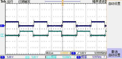
 At the EPWM2 I/O,  the PWM signal is normal.  However, at the Output Xbar I/O,  there doesn't exist signals.

After the button is pressed, the led can work normally, but the EPWM2 signal does not changed.

Where's the mistake of my code?

  • Chen,

    I will have to consult with PWM experts on this. Should be getting back to you shortly

    Regards,

    Peter

  • Chen,

    Before I consult with PWM experts, I will ask you to describe in some more detail what is your code intended to do. Specifically, please describe each step and tell us what is the intent and whether that particular step is working. When you get to the step that is not working, please explain to us what is the stimulus and what results were you expecting and what results you are getting.

    Thanks,

    Peter

  • Hi, Peter,

    Thanks for your reply.

    I have modified the description of my problem and added some explanation. I'm sure that the PWM module and GPIO module have been correctly set.

    I'm not sure about the CLB module and cannot figure out what the problem is.

  • Hi,

    I am contacting the CLB/PWM experts with this, should be getting back to you soon.


    REgards,

    PEter

  • Can you replace your OUTPUT XBAR functions with the driverlib version and try again?

    Same thing for the GPIO PinMux configuration for the output xbar.

  • Hi, Nima, 

    Thanks a lot for your help. I followed your advice but the problem still exist.

    I have made a vedio demonstrating how I creat the project and the experiment result.

    https://zhuanlan.zhihu.com/p/165997033

    According the experiment, the PWM module works normally and the led can change whenever the button is pressed.

    The detailed code is presented below. I still cannot find the problem. Could you help me ?

    #include "F28x_Project.h"     // Device Headerfile and Examples Include File
    
    #define DB_UP   1
    #define DB_DOWN 0
    
    void InitEPwm2Example(void);
    
    void main(void)
    {
        InitSysCtrl(); // system initial 200MHz
        InitGpio();
    
        InitEPwm1Gpio();   // GPIO0,1 is connected with two LED, and denotes the state of button
        InitEPwm2Gpio();    // EPWM2A,B is the generated PWM signals.
    
        //GPIO16 is set as I/O and is connected to a button.
        //When the button is pressed, the low level denotes the PWM faults
        //and the PWM signals should be blocked.
        GPIO_SetupPinMux(16,0,0);
        GPIO_SetupPinOptions(16, 0, GPIO_PULLUP);  //
    
        DINT;
    
        InitPieCtrl();
    
        IER = 0x0000;
        IFR = 0x0000;
    
        InitPieVectTable();
    
        //
        EALLOW;
        CpuSysRegs.PCLKCR0.bit.TBCLKSYNC =0;
        EDIS;
    
        InitEPwm2Example();
    
        EALLOW;
        CpuSysRegs.PCLKCR0.bit.TBCLKSYNC =1;
        EDIS;
    
        // -------   The code above can work normally.
        EALLOW;
        // Set GPIO16 as Input Xbar1
        XBAR_setInputPin(XBAR_INPUT1, 16);
    
        //Set InputXbar 1 as XBAR_AUXSIG0
        XBAR_setCLBMuxConfig(XBAR_AUXSIG0, XBAR_CLB_MUX01_INPUTXBAR1);
        XBAR_enableCLBMux(XBAR_AUXSIG0, XBAR_MUX01);
    
        EDIS;


        //Set GPIO14 as outputXbar 3
        GPIO_setPinConfig(GPIO_14_OUTPUTXBAR3);
        GPIO_setDirectionMode(14, GPIO_DIR_MODE_OUT);
        GPIO_setPadConfig(14, GPIO_PIN_TYPE_STD);
    
        // Set GPIO15 as  outputXbar 4
        GPIO_setPinConfig(GPIO_15_OUTPUTXBAR4);
        GPIO_setDirectionMode(15, GPIO_DIR_MODE_OUT);
        GPIO_setPadConfig(15, GPIO_PIN_TYPE_STD);
    
    
        // Set  CLB2_OUT4 as  outputXbar 3
        XBAR_setOutputMuxConfig(XBAR_OUTPUT3, XBAR_OUT_MUX05_CLB2_OUT4);
        XBAR_enableOutputMux(XBAR_OUTPUT3, XBAR_MUX05);
    
        //Set CLB2_OUT5 as outputXbar 4
        XBAR_setOutputMuxConfig(XBAR_OUTPUT4, XBAR_OUT_MUX07_CLB2_OUT5);
        XBAR_enableOutputMux(XBAR_OUTPUT4, XBAR_MUX07);
    
        //Let CLB_OUT6、7  substitute DB_PWM2A、B。
        CLB_setOutputMask(CLB2_BASE, 1 << 6 | 1 << 7, true);
    
        EDIS;


        // choose CLB2_BASE
        CLB_configLocalInputMux(CLB2_BASE, CLB_IN0, CLB_LOCAL_IN_MUX_GLOBAL_IN);
        CLB_configLocalInputMux(CLB2_BASE, CLB_IN1, CLB_LOCAL_IN_MUX_GLOBAL_IN);
        CLB_configLocalInputMux(CLB2_BASE, CLB_IN2, CLB_LOCAL_IN_MUX_GLOBAL_IN);
        CLB_configLocalInputMux(CLB2_BASE, CLB_IN3, CLB_LOCAL_IN_MUX_GLOBAL_IN);
        CLB_configLocalInputMux(CLB2_BASE, CLB_IN4, CLB_LOCAL_IN_MUX_GLOBAL_IN);
        CLB_configLocalInputMux(CLB2_BASE, CLB_IN5, CLB_LOCAL_IN_MUX_GLOBAL_IN);
        CLB_configLocalInputMux(CLB2_BASE, CLB_IN6, CLB_LOCAL_IN_MUX_GLOBAL_IN);
        CLB_configLocalInputMux(CLB2_BASE, CLB_IN7, CLB_LOCAL_IN_MUX_GLOBAL_IN);
    
    
        // GPIO16--> Input Xbar 1 -->  AUXSIG0  --> Boundary 0
        //                            EPWM2A_DB  --> Boundary 1
        //                            EPWM2B_DB  --> Boundary 2
        CLB_configGlobalInputMux(CLB2_BASE, CLB_IN0, CLB_GLOBAL_IN_MUX_CLB_AUXSIG0);
        CLB_configGlobalInputMux(CLB2_BASE, CLB_IN1, CLB_GLOBAL_IN_MUX_EPWM2A_DB);//
        CLB_configGlobalInputMux(CLB2_BASE, CLB_IN2, CLB_GLOBAL_IN_MUX_EPWM2B_DB);  //
        //
        CLB_configGlobalInputMux(CLB2_BASE, CLB_IN3, CLB_GLOBAL_IN_MUX_EPWM1A);
        CLB_configGlobalInputMux(CLB2_BASE, CLB_IN4, CLB_GLOBAL_IN_MUX_EPWM1A);
        CLB_configGlobalInputMux(CLB2_BASE, CLB_IN5, CLB_GLOBAL_IN_MUX_EPWM1A);
        CLB_configGlobalInputMux(CLB2_BASE, CLB_IN6, CLB_GLOBAL_IN_MUX_EPWM1A);
        CLB_configGlobalInputMux(CLB2_BASE, CLB_IN7, CLB_GLOBAL_IN_MUX_EPWM1A);
    
    
        // Select External for CLB2, IN0,1,2
        CLB_configGPInputMux(CLB2_BASE, CLB_IN0, CLB_GP_IN_MUX_EXTERNAL);
        CLB_configGPInputMux(CLB2_BASE, CLB_IN1, CLB_GP_IN_MUX_EXTERNAL);
        CLB_configGPInputMux(CLB2_BASE, CLB_IN2, CLB_GP_IN_MUX_EXTERNAL);
    
        CLB_configGPInputMux(CLB2_BASE, CLB_IN3, CLB_GP_IN_MUX_GP_REG);
        CLB_configGPInputMux(CLB2_BASE, CLB_IN4, CLB_GP_IN_MUX_GP_REG);
        CLB_configGPInputMux(CLB2_BASE, CLB_IN5, CLB_GP_IN_MUX_GP_REG);
        CLB_configGPInputMux(CLB2_BASE, CLB_IN6, CLB_GP_IN_MUX_GP_REG);
        CLB_configGPInputMux(CLB2_BASE, CLB_IN7, CLB_GP_IN_MUX_GP_REG);
    
        //Initial the CLB2 and Enable
        initTILE2(CLB2_BASE);
        CLB_enableCLB(CLB2_BASE);
    
        //EINT;  //
        ERTM;  //
    
        for(;;)
        {
    
            if (GpioDataRegs.GPADAT.bit.GPIO16 == 0)
            {
                GpioDataRegs.GPASET.bit.GPIO0 = 1;
                //   DELAY_US(100);
    
            }
            else
            {
                GpioDataRegs.GPACLEAR.bit.GPIO0 = 1;
                //   DELAY_US(100);
    
            }
    
            asm ("          NOP");
    
        }
    }


    void InitEPwm2Example()
    {
    
        EPwm2Regs.TBPRD = 5000;                       // Set timer period
        EPwm2Regs.TBPHS.bit.TBPHS = 0x0000;           // Phase is 0
        EPwm2Regs.TBCTR = 0x0000;                     // Clear counter
    
        // Setup TBCLK
        EPwm2Regs.TBCTL.bit.CTRMODE = TB_COUNT_UPDOWN; // Count up
        EPwm2Regs.TBCTL.bit.PHSEN = TB_DISABLE;        // Disable phase loading
        EPwm2Regs.TBCTL.bit.HSPCLKDIV = TB_DIV2;       // Clock ratio to SYSCLKOUT
        EPwm2Regs.TBCTL.bit.CLKDIV = TB_DIV1;          // Slow just to observe on the
        // scope
    
        // Setup compare
        EPwm2Regs.CMPA.bit.CMPA = 2500;
    
        // Set actions
        EPwm2Regs.AQCTLA.bit.CAU = AQ_SET;            // Set PWM2A on Zero
        EPwm2Regs.AQCTLA.bit.CAD = AQ_CLEAR;
    
        EPwm2Regs.AQCTLB.bit.CAU = AQ_CLEAR;          // Set PWM2A on Zero
        EPwm2Regs.AQCTLB.bit.CAD = AQ_SET;
    
        // Active Low complementary PWMs - setup the deadband
        EPwm2Regs.DBCTL.bit.OUT_MODE = DB_FULL_ENABLE;
        EPwm2Regs.DBCTL.bit.POLSEL = DB_ACTV_HIC;
        EPwm2Regs.DBCTL.bit.IN_MODE = DBA_ALL;
        EPwm2Regs.DBRED.bit.DBRED = 400;   // x*100 = delay x us
        EPwm2Regs.DBFED.bit.DBFED = 400;
        //EPwm2_DB_Direction = 1;
    
        // Interrupt where we will modify the deadband
        EPwm2Regs.ETSEL.bit.INTSEL = ET_CTR_ZERO;     // Select INT on Zero event
        EPwm2Regs.ETSEL.bit.INTEN = 1;                // Enable INT
        EPwm2Regs.ETPS.bit.INTPRD = ET_3RD;           // Generate INT on 3rd event
    
    }


  • You are overriding the EPWM2 output signals at the DEADBAND module. You also take in the signal from EPWM2 at the DEADBAND module. This is all good.

    You send the output to OUT4 and OUT5 and you take it out of the device using the OUTPUT XBAR which also looks correct.

    However, your CLB TILE is not functioning at all... You EPWM output comes out untouched, while your CLB OUT4 and OUT5 are always low...

    I'm not sure what the issue is. Can you start from a smaller example, like the AND gate ex8? We need to debug this step by step.

  • Did you try ex8 ?

  • Hi, Nima,

    I've tried the ex8

    I set EPWM3A (50% ducty cycle) as the input of GPIO0, V3.3 as the input of GPIO1. it is desired that the GPIO24 (outputxbar 1) should generate the EPWM3A waveform. However, the waveform holds low level. 

    This also shows that the CLB module did't work normally. Does this related to the hardware?   

    Could you try my code in the TI launchPads?

    Thanks a lot for your help.

  • Can you redo your project using DRIVERLIB only so I can test it on myside. I see some bitfields and I dont remember ever providing a Bitfield based CLB project.

    Can you update your project to be built on top of ex8? That way I can confirm that the issue is not comming from InitSysctl and other functions not originally tested with the Driverlib CLB examples.

    Nima

  • Hi,Nima

    Thanks a lot for your help. When I tried to modified the source code to use the  DRIVERLIB only, I found there exists two much inconvenience.

    Then,I realized that all the files that I used come from the C2000Ware shown by the vedio that I provided upside.

    And it is quite confusing that why there exists different lib for the same function, Just as I mentioned in the following post. 

    https://e2e.ti.com/support/microcontrollers/c2000/f/171/t/926319

     To find out the solution ,  I'll try to buy the TI launchPads and test the code. Thanks again for all your help

    Jianbo Chen

  • Thank you,

    Please let me know once completed.

    Nima