This thread has been locked.

If you have a related question, please click the "Ask a related question" button in the top right corner. The newly created question will be automatically linked to this question.

TMS320F28379D: Two memories on EMIF1 (One of them not working after while) [Flash/Mram]

Part Number: TMS320F28379D
Other Parts Discussed in Thread: C2000WARE

Hi, Im struggling with the problem that one of my memory (MRAM) stops working at irregular intervals after writing/reading (MRAM is completely damaged and it is no longer possible to work with it). I have multiple same circuits with new components (picture below), but after irregular intervals (a few days, one day or just one hour) MRAM stop working and is damaged for 100%. In my code, Im writing/reading from Mram every second from IPC or greater than one second depends on incoming different interrupts, possibly sometimes it can be every 400ms. Also I have Flash on same EMIF which performs the same cycle, but always after one minute, but it also depends on whether I get an interrupt so max. possible read/write cycle can occur every 1 second. I have done bool flags handling e.g in case, that an interrupt occurs and the program writes to mram it cannot write to Flash at sametime because im waiting before mram complete firstly, and if is everything done im clear flag and Flash can start or continue after IPC (Mram has higher priority in this case).

Specs:
MRAM: MR3A16AYS35
FLASH: S29GL128S90TFI010

So far I see the reason that on one of the flash pins will remain on (idk why), and the MRAM has a maximum output current on the pin only 20mA (Flash 100mA). Somehow some peak gets to the mram pin and it's over (But it is just my theory)... Could it be that you switch to the wrong or non-existing page? or not existing address or writing to non existing address ? As a driver im using example files emif_dc.c emif_dc.h edited for my gpios.

Have any of you already had a similar problem, or how could this issue be resolved? Thank very much for each suggestion and answer

Schematic (EM1CS3 is on GPIO35 not inc. in this picture)


  • Marek,

    Contention between memory components would be unusual because the EMIF provides arbitration of the CS/CE signals.

    One oddity that I am aware of is that the Flash RY/BY# signal takes a considerable amount of time (in EMIF terms) to become valid -- so the EMIF Extended Wait functionality may not work correctly if you configure the timings based on non-program operations. The flash example in C2000Ware handles this by polling on the RY/BY# signal using GPIO: ~\C2000Ware_XXXX\device_support\f2837xd\examples\cpu1\emif_dc_flash

    Are you able to determine which signal(s) might be damaged on the MRAM?  This might help to identify the cause.  It might be a good idea to scope the CS signals to make sure that they are reaching the expected voltage levels without overlap.

    Some minor observations from the schematics:

    • The GPIO72 switch is probably not  necessary -- a weak boot-strap pull resistor is not expected to degrade the EMIF functionality
    • EMIF1An functions can be used instead of EMIF1DQn for 16-b memories -- the UB/LB signals can be pulled down permanently because the C28x will always perform 16-b accesses
    • A17 is skipped on the MRAM

    -Tommy

  • Hello, thanks for fast reply. For Flash writing Im using EMIF_DC_programCS2Flash, but what I forgot to set up are these three variables:
    Should I set to the GPIO number or physical pin number on the processor? Could this be the cause? Because fuctionCS2Flash wait till EMIF_DC_FLASH_READY == 1 but its not for now...


    EDIT: (NVM, FLASH_READY pin is 36 like in photo, same for others...)

    For sector erase (chip erase).. Im using S29GLxxxS library, Erase will be performed when data need to be writen on new page of Flash, but when program start sector erase, and i got IPC to MRAM write and read can't it go crazy during this cycle?


    For MRAM, Im try only GPIO method with EMIF off, so I induced Word Read and Word Write states (in MRAM datasheet) only with gpio  turn on/off, Im wanted to write 1 0 1 0 1 0 .. sequence, but when i read it back i got only 0 0 0 0 0 0 on all EM1Dn pins (like in memory browser in CCS). So i dont really know what a specific pin was damaged.

    • When I didn't have this GPIO72 switch i cannot boot from standalone mode
    • Yes you are right, UB/LB can be pulled down
    • I know about that A17 is not connected (will be corrected in a new revision), but i hope that cannot cause this issue

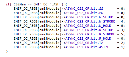
    I dont know if it help, but this is my MRAM and FLASH settings (emif on 100 MHz):
    MRAM


    FLASH

  • Marek Oravec said:
    For sector erase (chip erase).. Im using S29GLxxxS library, Erase will be performed when data need to be writen on new page of Flash, but when program start sector erase, and i got IPC to MRAM write and read can't it go crazy during this cycle?

    Yes, for special flash instructions that require additional wait cycles, you would want to hold-off MRAM accesses until the flash operation completes.

    Marek Oravec said:
    For MRAM, Im try only GPIO method with EMIF off, so I induced Word Read and Word Write states (in MRAM datasheet) only with gpio  turn on/off, Im wanted to write 1 0 1 0 1 0 .. sequence, but when i read it back i got only 0 0 0 0 0 0 on all EM1Dn pins (like in memory browser in CCS). So i dont really know what a specific pin was damaged.

    Can you check the voltage levels on the MRAM signal pins while progressing through the read and write sequences?

    Marek Oravec said:
    When I didn't have this GPIO72 switch i cannot boot from standalone mode

    It's ok to keep the switch, but if you were not able to boot with the pull resistor, it points to some potential contention at power up.  For example, the GPIO pins act as inputs during reset so the memory control signals are not biased by the F2837x during this time. It's possible that the memories may find themselves in an unintended read state where they drive output on the data bus.  This can be mitigated by installing pull-up resistors on the CS signals so that the devices will revert to a de-selected state when the CS signal is not actively controlled.

    Marek Oravec said:
    I dont know if it help, but this is my MRAM and FLASH settings (emif on 100 MHz)

    Nothing stands out to me as being problematic.  You can also use the EMIF configuration tool in C2000Ware to double-check your settings: ~\C2000Ware_XXXX\boards\TIDesigns\F28379D_EMIF_DC\C2000-EMIF_ConfigurationTool.xlsx

    There is also some usage information in this EMIF appnote.

  • Hello, I added some wait states when the flash chip/sector erasing. I added wait state also before MRAM write cycle. I hope it helps.

    #define FlashReadyStatus (GpioDataRegs.GPBDAT.bit.GPIO36) // Ready/Busy (Ready - 1 | Busy - 0)
    
    void lld_SectorEraseCmd
    (
    FLASHDATA * base_addr,                   /* device base address in system */
    ADDRESS offset                           /* address offset from base address */
    )
    { 
     
      /* Issue unlock sequence command */
      FLASH_WR(base_addr, LLD_UNLOCK_ADDR1, NOR_UNLOCK_DATA1);
      FLASH_WR(base_addr, LLD_UNLOCK_ADDR2, NOR_UNLOCK_DATA2);
    
      FLASH_WR(base_addr, LLD_UNLOCK_ADDR1, NOR_ERASE_SETUP_CMD);
      
      FLASH_WR(base_addr, LLD_UNLOCK_ADDR1, NOR_UNLOCK_DATA1);
      FLASH_WR(base_addr, LLD_UNLOCK_ADDR2, NOR_UNLOCK_DATA2);
    
      /* Write Sector Erase Command to Offset */
      FLASH_WR(base_addr, offset, NOR_SECTOR_ERASE_CMD);
    
      DELAY_US(1);
    
      while(FlashReadyStatus == 0); //Wait for Ready
    
    }

    I measured voltage levels also, during MRAM write/read cycle. Before Word Write,when E W are high, I have on these pins 3.18V - 3.25V. When i want to write my test sequence (1 0 1 0 ...) there is voltage 3.25V, 0V, 3.25V, 0V on data pins... But when i want to read it back i got 0V, 0V, 0V, 0V .... on Data pins. During Word Read i have only one pin high (W 3.25V) others are 0V as written in the datasheet...(I tested this program with good MRAM and when i readed it back i got 3.25V, 0V, 3.25V, 0V so no problem with my program.)

  • Marek,

    Your signal levels look ok.  At this point, I recommend a deeper dive into the MRAM requirements to see if some condition is being violated.

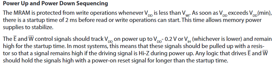
    For example, I noticed a power-up sequence in the MRAM datasheet that might need some attention:

    Maybe the MRAM is experiencing a dirty reset that would lead to unpredictable behavior.

    -Tommy

  • Tommy, thanks for advices. I soldered pull up resistors for E, W also for CS2, CS3 pins.I coded protection for memories with multiple state flags, so there are no possibility to write at once to flash or mram. Now, im going to burn program to processor and I will see if it helped. I will announce the result to this thread.

    Thank you so far.
  • Hello, after several days of hard testing I can say that the problem has been solved. I made additional treatments, so memories could not be met. Im also disable all interrupts when external flash writing or erasing, so that it does not jump out of the process..

    Summary:
    Added, "free chip monitoring" with flags (waiting before operations with flash/mram, if is CS3 or CS2 == 0)
    Added, waiting for Ready/Busy Flash pin (waiting before operations with mram, if is EM1WAIT (RY/BY) == 0)
    Added, interrupts disabling when flash writing or erasing process occured (DINT;..)
    Added, Pullup resistors for CS2, CS3, E, W

    Thank you for guidance Tommy, and I hope this thread will help someone with a similar problem.

    Best regards, Marek.

  • Marek,

    Good to hear that you have it working now.  Thanks for sharing your solution!

    -Tommy