This thread has been locked.

If you have a related question, please click the "Ask a related question" button in the top right corner. The newly created question will be automatically linked to this question.

TMS320F28374D: ADC issue in timing can you kindly check my test results and explain ?

Part Number: TMS320F28374D
Other Parts Discussed in Thread: C2000WARE

HI everybody , 

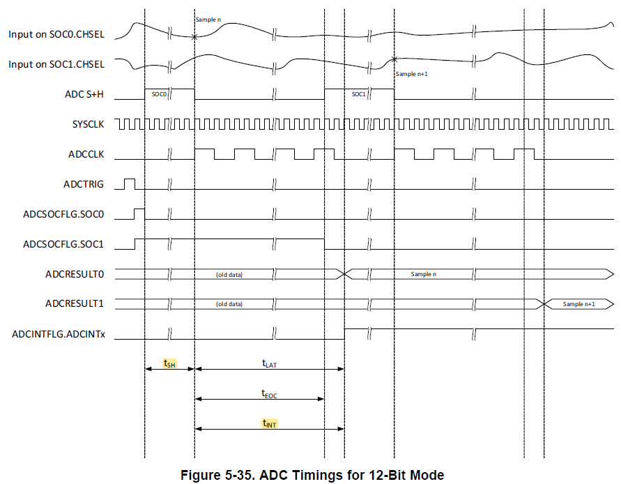
in attached  word you can see also code and scope screnshot , basically  adc timing does not match what expecting :

ADC TIMING Issues details :

Condition

  • SYSCLK is 200MHz, which is 5ns.


  • ePWM triggers ADC SOC at 40kHz period.


Code in attached word


  • Configured three ADC SOCs by using the same channel, ADCA CH_IN0.
    • To test I enabled only SOC0 first. And then, I enabled the rest of two to compare. When I did it, I also updated ADC_setInterruptSource to ADC_SOC_NUMBER0 or ADC_SOC_NUMBER2.


Code in attached word


  • Trigger ADC ISR at the end of SOC2
  • Using ADC DMA


Test

  • Trigger ADC ISR at the end of ADC SOC0
    • Yellow: PWM SYNC pulse
    • Blue:  ADC ISR Start
    • ADC Sampling time for SOC0 is 1us (S/H windows is set to 200, which will be 200 x 5ns = 1us)
    • The time between PWM SYNC pulse rising edge to the ADC ISR start point is about 1.42us. I did not include GPIO set time latency, but it looks the additional 420ns is longer than the value stated in the datasheet.


Scope in attached word


  • Trigger ADC ISR at the end of ADC SOC2
    • Yellow: PWM SYNC pulse
    • Blue:  ADC ISR Start
    • ADC Sampling time for SOC0 is 2.5us (please see the code above. S/H window is set to 500, which will be 500 x 5ns = 2.5us)
    • The time between PWM SYNC pulse rising edge to the ADC ISR start point is about 6.34us. This does not give me consistent result. I was expecting 2.5us + latency.


 thank you 

best regards

CarloADC TIMING Issues details.docx


  • Carlo,

    I see the intent of the measurements in the .docx, but there are a number of low-level details that are left out.  Did the measurement code start from an existing C2000Ware example?  Is this running on a TI board?

    -Tommy

  • tlee said:
    Did the measurement code start from an existing C2000Ware example?

    This would help a lot in making sure that the code base is good and I could then extract the low-level details from the examples.

    tlee said:
    Is this running on a TI board?

    Likewise, it would be easier to reproduce any issues using a TI board.

    tlee said:
    I see the intent of the measurements in the .docx, but there are a number of low-level details that are left out.

    For example, the .docx is assuming that the ADC conversion time is comprised solely of tSH, and ignores the tINT conversion and latch time.

    The tINT time is further dependent on the ADC prescale setting because there is a maximum supported ADC clock frequency:

    These factors need to be comprehended in the conversion time calculations.

    I also see in the .docx that the expected conversion time for a SOC2-generated interrupt is only considering the tSH for the SOC2 ACQPS, but the ADC appears to be configured to convert SOC0 -> SOC1 -> SOC2 so the tINT time needs to be calculated as the cumulative time for all three SOCs to complete.

  • Hi tlee,

    To answer your question:

    Did the measurement code start from an existing C2000Ware example?

    >> No, but pretty much following an example which uses API functions.

    Is this running on a TI board?

    >> Yes, it is running on the ControlCard.

    I have the following questions.

    • In the timing diagram, tLAT and tINT time are the same, but in the table, tLAT time is longer. 
    • 44 SYSCLK (200MHz) is 220ns.  
    • In the ADC configuration, the sample time between SOC is at least 500ns. So, I am not sure how tINT time is cumulated. Even though it is cumulated, 6us seems too long. Where can I find the information (e.g., timing diagram or etc.) and calculate the conversion and interrupt trigger time and verify with my board?

  • Justin Ryu1 said:
    In the timing diagram, tLAT and tINT time are the same, but in the table, tLAT time is longer.

    The timings in the table are accurate.  It would be appropriate to consider the diagram to be an abstracted model of behavior that shows the key state sequences.

    Justin Ryu1 said:
    In the ADC configuration, the sample time between SOC is at least 500ns. So, I am not sure how tINT time is cumulated. Even though it is cumulated, 6us seems too long. Where can I find the information (e.g., timing diagram or etc.) and calculate the conversion and interrupt trigger time and verify with my board?

    The timing diagram and table are meant to provide the basis for calculating ADC conversion times.  However, the calculations are influenced by a number of programmable behaviors that must be tracked down.

    From the limited information provided in the .docx, it looked like the ADC needed to execute all three SOCs before triggering the ADC interrupt.  This would have been 1100 cumulative S/H cycles (5.5us) + conversion time (possibly 220ns, depending on ADC configuration).

    I received some additional details offline that I will look into.

  • tlee said:
    I received some additional details offline that I will look into.

    It looks like the ADC prescale is configured for SYSCLK/4 with late interrupt so the tINT time should be 41 SYSCLK cycles.

    For a more precise latency measurement you can consider using the EPWM time base count to determine how many 100-MHz EPWM ticks elapsed from ADC trigger to ISR execution:

    adc_ticks = EPWM_getTimeBaseCounterValue(EPWM1_BASE) - EPWM_getCounterCompareValue(EPWM1_BASE, EPWM_COUNTER_COMPARE_A);

    If only SOC2 is intended to be profiled, the trigger settings for SOC0 and SOC1 should be changed so that they are not executed as a batch with SOC2.  By default, SOC0 and SOC1 will have higher priority.  Details of the SOC behavior can be found in the TRM.

  • tlee said:
    From the limited information provided in the .docx, it looked like the ADC needed to execute all three SOCs before triggering the ADC interrupt.  This would have been 1100 cumulative S/H cycles (5.5us) + conversion time (possibly 220ns, depending on ADC configuration).

    Correction on the math.  It would be:

    SOC0 = 5ns * (200 ACQPS + 41 tEOC) = 1.205us
    SOC1 = 5ns * (400 ACQPS + 41 tEOC) = 2.205us
    SOC2 = 5ns * (500 ACQPS + 41 tINT) = 2.705us

    SOC0 + SOC1 + SOC2 = 6.115us

  • I tested and verified it with cumulative SOC sampling time. I gave the sampling time like the following, to measure 1us, 2us, 3us.

    SOC0 = 5ns * (200 ACQPS + 41 tEOC) = 1.205us
    SOC1 = 5ns * (200 ACQPS + 41 tEOC) = 1.205us
    SOC2 = 5ns * (200 ACQPS + 41 tINT) = 1.205us

    SOC0 + SOC1 + SOC2 = 3.615us. 

    I measured the time from the scope, and it was 3.82us. GPIO assertion latency can be close to 200ns, I believe. 

    I also verified ADC voltage reading corresponding to the SOCs. 

    Thanks you!

  • Justin,

    Glad to hear that your measurements are closer to expectations now.

    -Tommy