


Part Number: LAUNCHXL-F28377S
Dear Community,
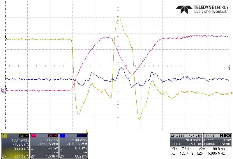
I got still a Problem with a correct switch off for PWM2A (and switch on for PWM2B) at the Moment when the analogue Comparator set his flag.
I use (PWM2B is the opposite):
-Zero-Events to switch on
-analogue Comp + Filter to set Flag
-a CBC-Event happen and pass through the digital Filter for a blanking-Window at the Beginn of the period
Is there in my Code a Issue by clearing the flags? Or is the Filter not correct?
The extra edges are alway about 20ns and this is the exact minimal time-periode for the PWM. (Maybe flagsare to early cleared or the filter is to short)
Or did a CBC-Event can happen every cycle (20ns) and than goes automatically low. I understnad that the CBC goes low after the whole period of the PWM.
to the picture:
yellow is PWM2A
red isPWM2B
blue is the analogue Signal for the Comp.
the Code:
everything I changed from the example of epwm_trip_zone
ignore pwm7
regards
//###########################################################################
//
// FILE:   epwm_trip_zone.c
//
// TITLE:  ePWM module using Trip-Zone submodule.
//
//! \addtogroup cpu01_example_list
//! <h1> EPWM Trip Zone Module (epwm_trip_zone)</h1>
//!
//! This example configures ePWM1 and ePWM2 as follows
//!  - ePWM1 has TZ1 as one shot trip source
//!  - ePWM2 has TZ1 as cycle by cycle trip source
//!
//! Initially tie TZ1 high. During the test, monitor ePWM1 or ePWM2
//! outputs on a scope. Pull TZ1 low to see the effect.
//!
//!  \b External \b Connections \n
//!  - EPWM1A is on GPIO0
//!  - EPWM2A is on GPIO2
//!  - TZ1 is on GPIO12
//!
//! This example also makes use of the Input X-BAR. GPIO12 (the external
//! trigger) is routed to the input X_BAR, from which it is routed to TZ1.
//!
//! The TZ-Event is defined such that EPWM1A will undergo a One-Shot Trip
//! and EPWM2A will undergo a Cycle-By-Cycle Trip.
//!
//              _____________             __________________
//              |           |             |                |
//  GPIO12 -----| I/P X-BAR |-----TZ1-----| ePWM TZ Module |-----TZ-Event
//              |___________|             |________________|
//
//
//
//###########################################################################
// $TI Release: F2837xS Support Library v210 $
// $Release Date: Tue Nov  1 15:35:23 CDT 2017 $
// $Copyright: Copyright (C) 2014-2017 Texas Instruments Incorporated -
//             http://www.ti.com/ ALL RIGHTS RESERVED $
//###########################################################################

//
// Included Files
//
#include "F28x_Project.h"

//
// Defines
//
#define EXTTrig     // Leave Uncommented for Testing with External Trigger.
                    // Comment for Testing with ePWM Trigger.
#define DB_UP          1

//definitions for selecting DACH reference
#define REFERENCE_VDDA     0
#define REFERENCE_VDAC     1
//definitions for COMPH input selection
#define NEGIN_DAC          0
#define NEGIN_PIN          1
//definitions for CTRIPH/CTRIPOUTH output selection
#define CTRIP_ASYNCH       0
#define CTRIP_SYNCH        1
#define CTRIP_FILTER       2
#define CTRIP_LATCH        3

//
// Globals
//
Uint32  EPwm7TZIntCount;
Uint32  EPwm2TZIntCount;
Uint16 EPwm2_DB_Direction;
Uint16 EPwm7_DB_Direction;


//
// Function Prototypes
//
//void InitEPwm7Example(void);
void InitEPwm2Example(void);
void InitEPwm7Example();
//raus gestrichen
//void InitTzGpio(void);
//__interrupt void epwm7_tzint_isr(void);
__interrupt void epwm2_tzint_isr(void);
__interrupt void epwm7_isr(void);
void InitEPwmGpio_TZ(void);
void InitCMPSS(void);

//
// Main
//
void main(void)
{
//
// Step 1. Initialize System Control:
// PLL, WatchDog, enable Peripheral Clocks
// This example function is found in the F2837xS_SysCtrl.c file.
//
    InitSysCtrl();

//
// Step 2. Initialize GPIO:
// This example function is found in the F2837xS_Gpio.c file and
// illustrates how to set the GPIO to it's default state.
//
    InitGpio();

//
// enable PWM1, and PWM2
//
    CpuSysRegs.PCLKCR2.bit.EPWM7=1;
    CpuSysRegs.PCLKCR2.bit.EPWM2=1;

//
// For this case just init GPIO pins for ePWM1, ePWM2, ePWM3
//
    InitEPwmGpio_TZ();
    //raus gestrichen
    //InitTzGpio();

//
// Step 3. Clear all interrupts and initialize PIE vector table:
// Disable CPU interrupts
//
    DINT;

//
// Initialize the PIE control registers to their default state.
// The default state is all PIE interrupts disabled and flags
// are cleared.
// This function is found in the F2837xS_PieCtrl.c file.
//
    InitPieCtrl();

//
// Disable CPU interrupts and clear all CPU interrupt flags:
//
    IER = 0x0000;
    IFR = 0x0000;

//
// Initialize the PIE vector table with pointers to the shell Interrupt
// Service Routines (ISR).
// This will populate the entire table, even if the interrupt
// is not used in this example.  This is useful for debug purposes.
// The shell ISR routines are found in F2837xS_DefaultIsr.c.
// This function is found in F2837xS_PieVect.c.
//
    InitPieVectTable();

//
// Interrupts that are used in this example are re-mapped to
// ISR functions found within this file.
//
    EALLOW; // This is needed to write to EALLOW protected registers
    //PieVectTable.EPWM7_TZ_INT = &epwm7_tzint_isr;
    PieVectTable.EPWM2_TZ_INT = &epwm2_tzint_isr;
    PieVectTable.EPWM7_TZ_INT = &epwm7_isr;
    EDIS;   // This is needed to disable write to EALLOW protected registers

//
// Step 4. Initialize the Device Peripherals:
//
    EALLOW;
    CpuSysRegs.PCLKCR0.bit.TBCLKSYNC =0;
    EDIS;

    InitEPwm7Example();
    InitEPwm2Example();
    // Configure Comparator COMP1H to accept POS input from pin and NEG input
    // from DAC
    //
    InitCMPSS();

    EALLOW;
    CpuSysRegs.PCLKCR0.bit.TBCLKSYNC =1;
    EDIS;

//
// Step 5. User specific code, enable interrupts:
//
    EPwm7TZIntCount = 0;
    EPwm2TZIntCount = 0;

//
// Enable CPU INT2 which is connected to EPWM1-3 INT:
//
    IER |= M_INT1;
    IER |= M_INT7;

//
// Enable EPWM INTn in the PIE: Group 3 interrupt 1-3
//
    PieCtrlRegs.PIEIER2.bit.INTx7 = 1;
    PieCtrlRegs.PIEIER2.bit.INTx2 = 1;

//
// Enable global Interrupts and higher priority real-time debug events:
//
    EINT;  // Enable Global interrupt INTM
    ERTM;  // Enable Global realtime interrupt DBGM

//
// Step 6. IDLE loop. Just sit and loop forever (optional):
//
    for(;;)
    {
        asm ("  NOP");
    }
}

//
// epwm1_tzint_isr - EPWM1 TZ ISR
//
/*__interrupt void epwm6_tzint_isr(void)
{
    EPwm6TZIntCount++;

    //
    // To Re-enable the OST Interrupt, do the following:
    // EALLOW;
    // EPwm1Regs.TZCLR.bit.OST = 1;
    // EPwm1Regs.TZCLR.bit.INT = 1;
    // EDIS;
    //

    //
    // Acknowledge this interrupt to receive more interrupts from group 2
    //
    PieCtrlRegs.PIEACK.all = PIEACK_GROUP2;
}
*/
//
// epwm2_tzint_isr - EPWM2 TZ ISR
//
__interrupt void epwm2_tzint_isr(void)
{
	//zusatz-->wird nicht gebraucht
    //GpioDataRegs.GPATOGGLE.bit.GPIO11 = 1;


    EPwm2TZIntCount++;

    //
    // Clear the flags - we will continue to take
    // this interrupt until the TZ pin goes high
    //
    EALLOW;
    //EPwm2Regs.TZCLR.bit.CBC = 1;
    //Löscht des CBC -Flag und es kann ein weiteres Interrupt erfolgen

    //besser wäre es den CBCPULSE zu nutzen
    //EPwm2Regs.TZCLR.bit.CBCPULSE = 0;

    //230218 wird nicht gebraucht
    //EPwm2Regs.TZCLR.bit.INT = 1;//Löschen des Interrupt-Flags des PWM-Moduls erlaubt das setzen weitere Interrupts

    EDIS;

    //
    // Acknowledge this interrupt to receive more interrupts from group 2
    //
    PieCtrlRegs.PIEACK.all = PIEACK_GROUP2;
}


//
// InitEPwm2Example - Initialize EPWM2 configuration
//
void InitEPwm2Example()
{
    //
    // Enable TZ1 as one cycle-by-cycle trip sources
    //
    EALLOW;
    //Für komplettes PWM-Modul
    ////260218
    //EPwm2Regs.TZSEL.bit.CBC1 = 1;

    //
    // Set TZA
    //für digital Compare
    //EPwm2Regs.TZCTL.bit.DCAEVT2= TZ_FORCE_LO;
    //
    //EPwm2Regs.TZCTL.bit.DCBEVT2 = TZ_FORCE_HI;

    //
    //nur für Trip
    EPwm2Regs.TZCTL.bit.TZA = TZ_FORCE_LO;
    //
    EPwm2Regs.TZCTL.bit.TZB = TZ_FORCE_HI;
    //
    // Enable TZ interrupt
    //
    //Für komplettes PWM-Modul
    //260218
    //EPwm2Regs.TZEINT.bit.CBC = 1;
    //260218
    EPwm2Regs.TZCLR.bit.CBCPULSE = 1;
    EDIS;

    EPwm2Regs.TBPRD = 499;//geändert von 250 auf 499, da hochgezäht wird (siehe Rechnung)                       // Set timer period
    EPwm2Regs.TBPHS.bit.TBPHS = 0x0000;           // Phase is 0
    EPwm2Regs.TBCTR = 0x0000;                     // Clear counter

    //
    // Setup TBCLK
    //
    EPwm2Regs.TBCTL.bit.CTRMODE = TB_COUNT_UP;//UP;//UPDOWN; // Count up
    EPwm2Regs.TBCTL.bit.PHSEN = TB_DISABLE;        // Disable phase loading
    EPwm2Regs.TBCTL.bit.HSPCLKDIV = TB_DIV1;//TB_DIV4;        // Clock ratio to SYSCLKOUT
    EPwm2Regs.TBCTL.bit.CLKDIV = TB_DIV1;//TB_DIV4;          // Slow just to observe on
                                                   // the scope.

    //
    // Setup compare
    //
    EPwm2Regs.CMPA.bit.CMPA = 490;

    // Set actions
    //
    EPwm2Regs.AQCTLB.bit.ZRO =AQ_CLEAR;
	EPwm2Regs.AQCTLA.bit.ZRO =AQ_SET;
	//2% der Endperiode ausgeschaltete PWM
	EPwm2Regs.AQCTLB.bit.CAU =AQ_SET;
	EPwm2Regs.AQCTLA.bit.CAU =AQ_CLEAR;

    // Set actions
    //
/*
    EPwm2Regs.AQCTLA.bit.CAU = AQ_CLEAR;             // Set PWM2A on CAU
    EPwm2Regs.AQCTLA.bit.CAD = AQ_SET;           // Clear PWM2A on CAD
    EPwm2Regs.AQCTLB.bit.CBU = AQ_SET; //Clear PWM2B on CAU
    EPwm2Regs.AQCTLB.bit.CBD = AQ_CLEAR;//Set PWM2B on CAD
*/

    /////////////////////////////////////////////////////////////////////////////////
    //Hinzufügen der Deadband Einstellungen
    //Dreht alle PWm EInstellungen um
        // Active Low complementary PWMs - setup the deadband
        //
        //EPwm2Regs.DBCTL.bit.OUT_MODE = DB_FULL_ENABLE;
        //EPwm2Regs.DBCTL.bit.POLSEL = DB_ACTV_HIC;//DB_ACTV_LOC;
        //EPwm2Regs.DBCTL.bit.IN_MODE = DBA_ALL;
        //EPwm2Regs.DBRED.bit.DBRED = 8;//EPWM2_MIN_DB;
        //EPwm2Regs.DBFED.bit.DBFED = 8;//EPWM2_MIN_DB;
        //EPwm2_DB_Direction = DB_UP;
        //
        // Interrupt where we will modify the deadband
        //
        //EPwm2Regs.ETSEL.bit.INTSEL = ET_CTR_ZERO;     // Select INT on Zero event
       // EPwm2Regs.ETSEL.bit.INTEN = 1;                // Enable INT
        //EPwm2Regs.ETPS.bit.INTPRD = ET_3RD;           // Generate INT on 3rd event
        //////////////////////////////////////////////////////////////////////////
//Einstellungen für die Weiterleitung aus der x-Bar ins Trip-Zone-Sub-Modul
/////////////////////////////////////////////////////////////////////////////////
        EALLOW;
        //
        //Configure DCB to be TRIP4
        //
        //EPwm8Regs.TZDCSEL.bit.DCBEVT1 = TZ_DCBH_HI;
        EPwm2Regs.TZDCSEL.bit.DCBEVT2 = TZ_DCBH_HI;//Abänderung in CBC
        //Hier kann noch die Polarität eingestellt werden und was so passiert

        //EPwm8Regs.DCTRIPSEL.bit.DCBHCOMPSEL = 0xF;
        EPwm2Regs.DCTRIPSEL.bit.DCBHCOMPSEL = 3;//0xF;//kann so bleiben alle Trips sind aktiv-->3 nur Trip 4 ist aktiv
        //EPwm8Regs.DCBHTRIPSEL.bit.TRIPINPUT4 = 1;
        EPwm2Regs.DCBHTRIPSEL.bit.TRIPINPUT4 = 1; //Input 1 selected as combinational ORed input to DCBH mux

        //
        //Configure DCB as OST
        //
        //EPwm8Regs.TZSEL.bit.DCBEVT1 = 1;
        //Enable DCBEVT2 as a CBC trip source for this ePWM module

        EPwm2Regs.TZSEL.bit.DCBEVT2 = 1;//Abänderung in CBC
        //Erweiterung um A
        //EPwm2Regs.TZSEL.bit.DCAEVT2 = 1;
        //noch möglich --> Enable TZ1 as a CBC trip source for this ePWM module

        //
        //Configure DCB path to be unfiltered & async
        //
        //EPwm8Regs.DCBCTL.bit.EVT1SRCSEL = DC_EVT1;
        EPwm2Regs.DCBCTL.bit.EVT2SRCSEL = 1;//Auskommentierung und 1 gesetzt; Filtereingang statt Event Eingang ;DC_EVT2;//Abänderung in CBC
        //Erweiterung um A
        //EPwm2Regs.DCACTL.bit.EVT2SRCSEL = DC_EVT2;
        //EPwm8Regs.DCBCTL.bit.EVT1FRCSYNCSEL = DC_EVT_ASYNC;
        EPwm2Regs.DCBCTL.bit.EVT2FRCSYNCSEL = DC_EVT_SYNC; //Abänderung in CBC und in Syncorn zur TBCLK-->keine Probleme im Deadband
        //Erweiterung um A
        //EPwm2Regs.DCACTL.bit.EVT2FRCSYNCSEL = DC_EVT_ASYNC;

        CpuSysRegs.PCLKCR0.bit.TBCLKSYNC = 1;

        //
        //Configure TRIP4 to be CTRIP1H
        //
        EPwmXbarRegs.TRIP4MUX0TO15CFG.bit.MUX0 = 0;

        //
        //Enable TRIP4 Mux for Output
        //
        EPwmXbarRegs.TRIP4MUXENABLE.bit.MUX0 = 1;

        //
        // Clear trip flags
        //
        //EPwm8Regs.TZCLR.bit.OST = 1;

        //230218 wird nicht gebraucht
        //EPwm2Regs.TZCLR.bit.DCBEVT2 = 1;

        //Erweiterung um A
        //EPwm2Regs.TZCLR.bit.DCAEVT2 = 1;
        //EPwm8Regs.TZCLR.bit.INT = 1;

        //230218 wird nicht gebraucht
        //EPwm2Regs.TZCLR.bit.INT = 1;

        //NOTE: No further EPWMx_TZINT PIE interrupts will be generated
        //until the flag is cleared. If the TZFLG[INT] bit is cleared and any of
        //the other flag bits are set, then another interrupt pulse will be
        //generated. Clearing all flag bits will prevent further interrupts.

        //
        //Enable DCB interrupt
        //
        //EPwm8Regs.TZEINT.bit.OST = 1;

        //230218 wird nicht gebraucht
        //EPwm2Regs.TZEINT.bit.DCBEVT2 = 1;

        //Erweiterung um A
        //EPwm2Regs.TZEINT.bit.DCAEVT2 = 1;
/////////////////////////////////////////////////////////////////////////////////

        //Hinzufügen des Blanking
        EPwm2Regs.DCFCTL.bit.BLANKE= 1;//Aktiviert Blanking-Window
        EPwm2Regs.DCFCTL.bit.PULSESEL=1; //Startet mit Zero
        EPwm2Regs.DCFCTL.bit.SRCSEL=3; //Filter Block Signal Aussuchen --> DCBEVT2
        EPwm2Regs.DCFOFFSET=0;//1960; //Fenster wird null TBCLK von PRD statt finden alternativ geht auch CTR
        EPwm2Regs.DCFWINDOW=20;//Setzen eines Blanking Fenster mit 40 = 200ns --> 200Mhz = 5e-9 --> 40 * 5e-9 = 200ns

////////////////////////////////////////////////////////////////////////////////
        EDIS;

}

//
// InitTzGpio - Initialize TZ GPIOs
//
/*
void InitTzGpio(void)
{
    //
    // For External Trigger, GPIO12 as the trigger for TripZone
    //
    GpioCtrlRegs.GPAPUD.bit.GPIO12 = 0;    // Enable pull-up on GPIO12 (TZ1)

    GpioCtrlRegs.GPAQSEL1.bit.GPIO12 = 3;  // Asynch input GPIO12 (TZ1)

    EALLOW;
    InputXbarRegs.INPUT1SELECT = 12;
    EDIS;

    //
    // For monitoring when the TZ Interrupt has been entered
    //

}
*/

//
// InitEPwmGpio_TZ - Initialize EPWM1A and EPWM2A GPIOs
//
void InitEPwmGpio_TZ(void)
{
    EALLOW;
    GpioCtrlRegs.GPAPUD.bit.GPIO2 = 1;    // Disable pull-up on GPIO2 (EPWM2A)
    GpioCtrlRegs.GPAMUX1.bit.GPIO2 = 1;   // Configure GPIO2 as EPWM2A
    GpioCtrlRegs.GPAPUD.bit.GPIO3 = 1;    // Disable pull-up on GPIO3 (EPWM2B)
    GpioCtrlRegs.GPAMUX1.bit.GPIO3 = 1;   // Configure GPIO3 as EPWM2B

    GpioCtrlRegs.GPAPUD.bit.GPIO12 = 1;    // Disable pull-up on GPIO10 (EPWM7A)
    GpioCtrlRegs.GPAMUX1.bit.GPIO12 = 1;   // Configure GPIO10 as EPWM7A
    GpioCtrlRegs.GPAPUD.bit.GPIO13 = 1;    // Disable pull-up on GPIO11 (EPWM7B)
    GpioCtrlRegs.GPAMUX1.bit.GPIO13 = 1;   // Configure GPIO11 as EPWM7B
    EDIS;
}

//
// End of file
//

//
// InitCMPSS - Initialize CMPSS1 and configure settings
//
void InitCMPSS(void)
{
    EALLOW;

    //
    //Enable CMPSS
    //
    Cmpss1Regs.COMPCTL.bit.COMPDACE = 1;

    //
    //NEG signal comes from DAC
    //
    Cmpss1Regs.COMPCTL.bit.COMPHSOURCE = NEGIN_DAC;

    //
    //Use VDDA as the reference for DAC
    //
    Cmpss1Regs.COMPDACCTL.bit.SELREF = REFERENCE_VDDA;

    //
    //Set DAC to midpoint for arbitrary reference
    //
    Cmpss1Regs.DACHVALS.bit.DACVAL = 1048;

    //
    // Configure CTRIPOUT path
    // Asynch output feeds CTRIPH and CTRIPOUTH
    //
    Cmpss1Regs.COMPCTL.bit.CTRIPHSEL = CTRIP_ASYNCH;
    //Cmpss1Regs.COMPCTL.bit.CTRIPOUTHSEL = CTRIP_ASYNCH;

    //
    // Configure CTRIPOUTH output pin
    // Configure OUTPUTXBAR3 to be CTRIPOUT1H
    //
    //OutputXbarRegs.OUTPUT3MUX0TO15CFG.bit.MUX0 = 0;

    //
    //Enable OUTPUTXBAR3 Mux for Output
    //
    //OutputXbarRegs.OUTPUT3MUXENABLE.bit.MUX0 = 1;

/////////////////////////////////////////////////////////////////////////////////
//Filter für Comparator
    Cmpss1Regs.CTRIPHFILCTL.bit.SAMPWIN=15; //Es müssen 6 Samples +Sample high sein zum Durschalten
    Cmpss1Regs.CTRIPHFILCTL.bit.THRESH=13; //Die Mehrheit also 4-Abtasttung müssen wenigstens high sein
    Cmpss1Regs.CTRIPHFILCLKCTL.bit.CLKPRESCALE=4; //2-->es wird nur jede zweite Periode ein Sample generriert (system clk)
    Cmpss1Regs.CTRIPHFILCTL.bit.FILINIT=1;//Aktivierung des zusätzlichen Filters
    Cmpss1Regs.COMPSTSCLR.bit.HSYNCCLREN=1;

    /////////////////////////////////////////////////////////////////////////////////
    EDIS;
}


void InitEPwm7Example()
{
	EALLOW;

    EPwm7Regs.TBPRD = 250;                       // Set timer period
    EPwm7Regs.TBPHS.bit.TBPHS = 0x0000;           // Phase is 0
    EPwm7Regs.TBCTR = 0x0000;                     // Clear counter
    //
    // Setup TBCLK
    //
    EPwm7Regs.TBCTL.bit.CTRMODE = TB_COUNT_UPDOWN; // Count up
    EPwm7Regs.TBCTL.bit.PHSEN = TB_DISABLE;        // Disable phase loading
    EPwm7Regs.TBCTL.bit.HSPCLKDIV = TB_DIV1;       // Clock ratio to SYSCLKOUT//am ende von 4 auf 1 geandert
    EPwm7Regs.TBCTL.bit.CLKDIV = TB_DIV1;          // Slow just to observe on
                                                   // the scope
    //
    // Setup compare
    //
    //EPwm2Regs.CMPA.bit.CMPA = 125;
//Anpassung auf Regeler
    EPwm7Regs.CMPA.bit.CMPA = 10;
    //EPwm7Regs.CMPB.bit.CMPB = 125;
    //
    // Set actions
    //
    //EPwm7Regs.AQCTLB.bit.ZRO =AQ_CLEAR;
	EPwm7Regs.AQCTLA.bit.ZRO =AQ_SET;
    //EPwm7Regs.AQCTLA.bit.CAU = AQ_SET;            // Set PWM2A on Zero
    EPwm7Regs.AQCTLA.bit.CAD = AQ_CLEAR;
    //EPwm7Regs.AQCTLB.bit.CAU = AQ_CLEAR;          // Set PWM2A on Zero
    //EPwm7Regs.AQCTLB.bit.CAD = AQ_SET;
    //
    // Active Low complementary PWMs - setup the deadband
    //

    EPwm7Regs.DBCTL.bit.OUT_MODE = DB_FULL_ENABLE;
    EPwm7Regs.DBCTL.bit.POLSEL = DB_ACTV_HIC;//DB_ACTV_LOC;
    EPwm7Regs.DBCTL.bit.IN_MODE = DBA_ALL;
    EPwm7Regs.DBRED.bit.DBRED = 2;//EPWM2_MIN_DB;
    EPwm7Regs.DBFED.bit.DBFED = 2;//EPWM2_MIN_DB;
    EPwm7_DB_Direction = DB_UP;
    //
    // Interrupt where we will modify the deadband
    //


    EPwm7Regs.ETSEL.bit.INTSEL = ET_CTR_ZERO;     // Select INT on Zero event
    EPwm7Regs.ETSEL.bit.INTEN = 1;                // Enable INT
    EPwm7Regs.ETPS.bit.INTPRD = ET_3RD;           // Generate INT on 3rd event
    EDIS;
}
__interrupt void epwm7_isr(void)
{

    EPwm7Regs.ETCLR.bit.INT = 1;

}

