This thread has been locked.

If you have a related question, please click the "Ask a related question" button in the top right corner. The newly created question will be automatically linked to this question.

CCS/TMS320F28377S: The data read from flash isn't correct

Part Number: TMS320F28377S
Other Parts Discussed in Thread: C2000WARE

Tool/software: Code Composer Studio

Hi,

I read the data from the flash. But the data isn't correct. The following is the function that read data from Section Z.

#pragma CODE_SECTION(Flash_Read, "ramfuncs");
void Flash_Read(uint16 *Reci_Buffer)
{
uint8 i;

uint16 *Reci_Buffer32=(uint16 *)Bzero_SectorZ_start;

uint16 Reci_Data;

for(i=0;i<=WORDS_IN_FLASH_BUFFER;i++){
Reci_Data=*(Reci_Buffer32+i);
*(Reci_Buffer+i)=Reci_Data;
}

}

The value of *(Reci_Buffer32+i) is 0xffff that can display in watch windows. But the Reci_Data is change to 0x7fff. I don't know the reason why cause this issue. I appreciate if you can give me some suggestion. Thanks.

  • Hi - What is the system frequency and wait state configuration for Flash?

    Regards,
    Nirav
  • The system frequency is 200Mhz. You can see the value of *(Reci_Buffer32+i) from Watch windows is 0xffff that is the same value in the memory windows. The address is 0xfa002. That means the data is successful reading from flash. The issue is the variable Reci_Data on the left expression can't get the value on the right expression. it's so weird. 

    BTW, The data read from 0xfa000,0xfa001 and 0xfa003 are correct and Reci_data can also get these correct value. thanks

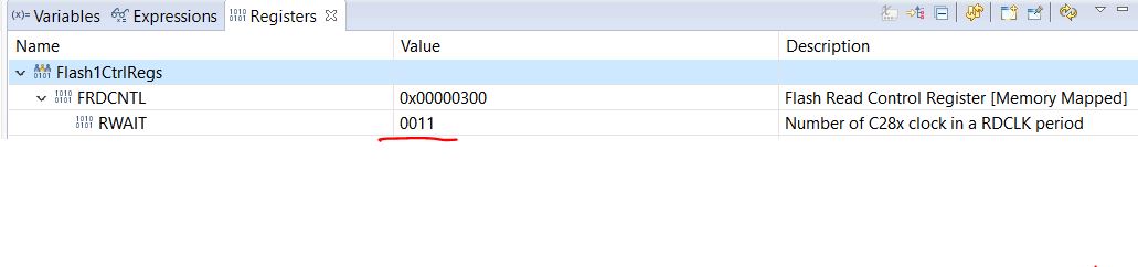
  • What is the RWAIT configuration inside FRDCNTL register? Can you make sure you have configured the value of at least "3"?

    It is possible if RWAIT is not configured to the minimum required value as per the data sheet, then you are reading data early and hence the value in "Reci_data" is not correct. Now when you look at the expression *(Reci_Buffer32+i) in watch window it gets evaluated multiple time, and hence the value that you read is correct since the data becomes available when you do multiple reads.

    Regards,
    Nirav
  • Hi Nirav,

    Thanks for your reply. The RWAIT in FRDCNTL register was "3".  The "Reci_data" can got the correct value 0xffff when I debug with step by step. But the "Reci_data" will get wrong value 0x7fff when I run the program without any breakpoints.  I appreciate if you can give me more help. thanks.

    BTW, The same issue will happen when I changed RWAIT to "0x6" or the maximum value "0xf". Thanks

  • Hi John,

    Couple of things that you can try out:

    1. What is the OSCCLKSRC for the PLL is it XTAL or INTOSC1/2? If it is INTOSC1/2 you need to add one more wait state i.e. RWAIT=4.

    2. Are you enabling pre-fetch or data cache? Can you dump FRD_INTF_CTRL register content?

    Regards,
    Nirav
  • Hi Nirav,

    I set RWAIT to "4" and set the DATA_CACHE_EN and PREFETCH_EN to "0". But the issue is still exist. The debug step by step is working fine. The running without any breakpoints will get wrong value. 

  • Hi John,

    Can you try reducing the System Clock frequency to 194Mhz if you are using INTOSC1/INTOSC2 as the clock source for the PLL? As per the spec, if INTOSC1/2 is used as the OSCCLKSRC the max device frequency is 194MHz.

    You can use RWAIT=3 when you lower the frequency to 194MHz.

    Regards,
    Nirav
  • HI Nirav,

    I don't use INTOSC1/INTOSC2 as the clock source. I used a 10Mhz external crystal as clock source. Thanks.

    Regards,

    John

  • Hi John,

    Ok, in that case you can run the SYSCLK at 200MHz. Are you seeing incorrect values for all the addresses that you read or only for 0xFA000? If you do not mind can you send the snippet of the code from beginning where you initialize the device (PLL, SYSCLK etc.).

    Thanks,
    Nirav
  • Hi Nirav,

    The enclose the source code of system initialisation. The first line in main() is InitSysCtrl(); which is inside of file F2837xS_SysCtrl.c. Thanks.

    Regards,

    John

    //###########################################################################
    //
    // FILE:   F2837xS_SysCtrl.c
    //
    // TITLE:  F2837xS Device System Control Initialization & Support Functions.
    //
    // DESCRIPTION:
    //
    //         Example initialization of system resources.
    //
    //###########################################################################
    // $TI Release: F2837xS Support Library v180 $
    // $Release Date: Fri Nov  6 16:27:58 CST 2015 $
    // $Copyright: Copyright (C) 2014-2015 Texas Instruments Incorporated -
    //             http://www.ti.com/ ALL RIGHTS RESERVED $
    //###########################################################################
    
    #include "F2837xS_device.h"     // Headerfile Include File
    #include "F2837xS_Examples.h"   // Examples Include File
    
    // Functions that will be run from RAM need to be assigned to
    // a different section.  This section will then be mapped to a load and
    // run address using the linker cmd file.
    //
    //  *IMPORTANT*
    //  IF RUNNING FROM FLASH, PLEASE COPY OVER THE SECTION "ramfuncs"  FROM FLASH
    //  TO RAM PRIOR TO CALLING InitSysCtrl(). THIS PREVENTS THE MCU FROM THROWING
    //  AN EXCEPTION WHEN A CALL TO DELAY_US() IS MADE. 
    //
    
    #define _LAUNCHXL_F28377S
    
    #pragma CODE_SECTION(InitFlash_Bank0, "ramfuncs");
    #pragma CODE_SECTION(InitFlash_Bank1, "ramfuncs");
    #pragma CODE_SECTION(FlashOff_Bank0, "ramfuncs");
    #pragma CODE_SECTION(FlashOff_Bank1, "ramfuncs");
    
    void InitSysCtrl(void)
    {
        // Disable the watchdog
        DisableDog();
    
    #ifdef _FLASH
    // Copy time critical code and Flash setup code to RAM
    // This includes the following functions:  InitFlash();
    // The  RamfuncsLoadStart, RamfuncsLoadSize, and RamfuncsRunStart
    // symbols are created by the linker. Refer to the device .cmd file.
        memcpy(&RamfuncsRunStart, &RamfuncsLoadStart, (size_t)&RamfuncsLoadSize);
    
    // Call Flash Initialization to setup flash waitstates
    // This function must reside in RAM
        InitFlash_Bank0();
        InitFlash_Bank1();
    #endif
    
        // *IMPORTANT*
        // The Device_cal function, which copies the ADC & oscillator calibration values
        // from TI reserved OTP into the appropriate trim registers, occurs automatically
        // in the Boot ROM. If the boot ROM code is bypassed during the debug process, the
        // following function MUST be called for the ADC and oscillators to function according
        // to specification. The clocks to the ADC MUST be enabled before calling this
        // function.
        // See the device data manual and/or the ADC Reference
        // Manual for more information.
    
        EALLOW;
    
        //enable pull-ups on unbonded IOs as soon as possible to reduce power consumption.
        GPIO_EnableUnbondedIOPullups();
    
    	CpuSysRegs.PCLKCR13.bit.ADC_A = 1;
    	CpuSysRegs.PCLKCR13.bit.ADC_B = 1;
    	CpuSysRegs.PCLKCR13.bit.ADC_C = 1;
    	CpuSysRegs.PCLKCR13.bit.ADC_D = 1;
    
        //check if device is trimmed
        if(*((Uint16 *)0x5D1B6) == 0x0000){
            //device is not trimmed, apply static calibration values
            AnalogSubsysRegs.ANAREFTRIMA.all = 31709;
            AnalogSubsysRegs.ANAREFTRIMB.all = 31709;
            AnalogSubsysRegs.ANAREFTRIMC.all = 31709;
            AnalogSubsysRegs.ANAREFTRIMD.all = 31709;
        }
    
    	CpuSysRegs.PCLKCR13.bit.ADC_A = 0;
    	CpuSysRegs.PCLKCR13.bit.ADC_B = 0;
    	CpuSysRegs.PCLKCR13.bit.ADC_C = 0;
    	CpuSysRegs.PCLKCR13.bit.ADC_D = 0;
        EDIS;
    
        // Initialize the PLL control: PLLCR and CLKINDIV
        // F28_PLLCR and F28_CLKINDIV are defined in F2837xS_Examples.h
        // Note: The internal oscillator CANNOT be used as the PLL source if the
        // PLLSYSCLK is configured to frequencies above 194 MHz.
    
        //InitSysPll(XTAL_OSC,IMULT_20,FMULT_1,PLLCLK_BY_2);
        //PLLSYSCLK = 10Mhz(OSCCLK) * 40 (IMULT) * 1 (FMULT) /  2 (PLLCLK_BY_2)      200Mhz
        //PLLSYSCLK = 10Mhz(OSCCLK) * 20 (IMULT) * 1 (FMULT) /  2 (PLLCLK_BY_2)      100Mhz
    
    #ifdef _LAUNCHXL_F28377S
        InitSysPll(XTAL_OSC,IMULT_40,FMULT_0,PLLCLK_BY_2); 		//PLLSYSCLK = (XTAL_OSC) * (IMULT + FMULT) / (PLLSYSCLKDIV)
    #else
        InitSysPll(XTAL_OSC,IMULT_20,FMULT_0,PLLCLK_BY_2); 		//PLLSYSCLK = (XTAL_OSC) * (IMULT + FMULT) / (PLLSYSCLKDIV)
    #endif
    
        //Turn on all peripherals
    	InitPeripheralClocks();
    
    }
    
    //---------------------------------------------------------------------------
    // InitPeripheralClocks
    //---------------------------------------------------------------------------
    // This function initializes the clocks for the peripherals. 
    //
    // Note: In order to reduce power consumption, turn off the clocks to any 
    // peripheral that is not specified for your part-number or is not used in the 
    // application
    void InitPeripheralClocks()
    {
    	EALLOW;
    
    	CpuSysRegs.PCLKCR0.bit.CLA1 = 1;
    	CpuSysRegs.PCLKCR0.bit.DMA = 1;
    	CpuSysRegs.PCLKCR0.bit.CPUTIMER0 = 1;
    	CpuSysRegs.PCLKCR0.bit.CPUTIMER1 = 1;
    	CpuSysRegs.PCLKCR0.bit.CPUTIMER2 = 1;
    	CpuSysRegs.PCLKCR0.bit.HRPWM = 1;
    	CpuSysRegs.PCLKCR0.bit.TBCLKSYNC = 1;
    
    	CpuSysRegs.PCLKCR1.bit.EMIF1 = 1;
    	CpuSysRegs.PCLKCR1.bit.EMIF2 = 1;
    
    	CpuSysRegs.PCLKCR2.bit.EPWM1 = 1;
    	CpuSysRegs.PCLKCR2.bit.EPWM2 = 1;
    	CpuSysRegs.PCLKCR2.bit.EPWM3 = 1;
    	CpuSysRegs.PCLKCR2.bit.EPWM4 = 1;
    	CpuSysRegs.PCLKCR2.bit.EPWM5 = 1;
    	CpuSysRegs.PCLKCR2.bit.EPWM6 = 1;
    	CpuSysRegs.PCLKCR2.bit.EPWM7 = 1;
    	CpuSysRegs.PCLKCR2.bit.EPWM8 = 1;
    	CpuSysRegs.PCLKCR2.bit.EPWM9 = 1;
    	CpuSysRegs.PCLKCR2.bit.EPWM10 = 1;
    	CpuSysRegs.PCLKCR2.bit.EPWM11 = 1;
    	CpuSysRegs.PCLKCR2.bit.EPWM12 = 1;
    
    	CpuSysRegs.PCLKCR3.bit.ECAP1 = 1;
    	CpuSysRegs.PCLKCR3.bit.ECAP2 = 1;
    	CpuSysRegs.PCLKCR3.bit.ECAP3 = 1;
    	CpuSysRegs.PCLKCR3.bit.ECAP4 = 1;
    	CpuSysRegs.PCLKCR3.bit.ECAP5 = 1;
    	CpuSysRegs.PCLKCR3.bit.ECAP6 = 1;
    
    	CpuSysRegs.PCLKCR4.bit.EQEP1 = 1;
    	CpuSysRegs.PCLKCR4.bit.EQEP2 = 1;
    	CpuSysRegs.PCLKCR4.bit.EQEP3 = 1;
    
    	CpuSysRegs.PCLKCR6.bit.SD1 = 1;
    	CpuSysRegs.PCLKCR6.bit.SD2 = 1;
    
    	CpuSysRegs.PCLKCR7.bit.SCI_A = 1;
    	CpuSysRegs.PCLKCR7.bit.SCI_B = 1;
    	CpuSysRegs.PCLKCR7.bit.SCI_C = 1;
    	CpuSysRegs.PCLKCR7.bit.SCI_D = 1;
    
    	CpuSysRegs.PCLKCR8.bit.SPI_A = 1;
    	CpuSysRegs.PCLKCR8.bit.SPI_B = 1;
    	CpuSysRegs.PCLKCR8.bit.SPI_C = 1;
    
    	CpuSysRegs.PCLKCR9.bit.I2C_A = 1;
    	CpuSysRegs.PCLKCR9.bit.I2C_B = 1;
    
    	CpuSysRegs.PCLKCR10.bit.CAN_A = 1;
    	CpuSysRegs.PCLKCR10.bit.CAN_B = 1;
    
    	CpuSysRegs.PCLKCR11.bit.McBSP_A = 1;
    	CpuSysRegs.PCLKCR11.bit.McBSP_B = 1;
    	CpuSysRegs.PCLKCR11.bit.USB_A = 1;
    
    	CpuSysRegs.PCLKCR12.bit.uPP_A = 1;
    
    	CpuSysRegs.PCLKCR13.bit.ADC_A = 1;
    	CpuSysRegs.PCLKCR13.bit.ADC_B = 1;
    	CpuSysRegs.PCLKCR13.bit.ADC_C = 1;
    	CpuSysRegs.PCLKCR13.bit.ADC_D = 1;
    
    	CpuSysRegs.PCLKCR14.bit.CMPSS1 = 1;
    	CpuSysRegs.PCLKCR14.bit.CMPSS2 = 1;
    	CpuSysRegs.PCLKCR14.bit.CMPSS3 = 1;
    	CpuSysRegs.PCLKCR14.bit.CMPSS4 = 1;
    	CpuSysRegs.PCLKCR14.bit.CMPSS5 = 1;
    	CpuSysRegs.PCLKCR14.bit.CMPSS6 = 1;
    	CpuSysRegs.PCLKCR14.bit.CMPSS7 = 1;
    	CpuSysRegs.PCLKCR14.bit.CMPSS8 = 1;
    
    	CpuSysRegs.PCLKCR16.bit.DAC_A = 1;
    	CpuSysRegs.PCLKCR16.bit.DAC_B = 1;
    	CpuSysRegs.PCLKCR16.bit.DAC_C = 1;
    	
    	EDIS;
    }
    
    void DisablePeripheralClocks()
    {
    	EALLOW;
    
    	CpuSysRegs.PCLKCR0.all = 0;
    	CpuSysRegs.PCLKCR1.all = 0;
    	CpuSysRegs.PCLKCR2.all = 0;
    	CpuSysRegs.PCLKCR3.all = 0;
    	CpuSysRegs.PCLKCR4.all = 0;
    	CpuSysRegs.PCLKCR6.all = 0;
    	CpuSysRegs.PCLKCR7.all = 0;
    	CpuSysRegs.PCLKCR8.all = 0;
    	CpuSysRegs.PCLKCR9.all = 0;
    	CpuSysRegs.PCLKCR10.all = 0;
    	CpuSysRegs.PCLKCR11.all = 0;
    	CpuSysRegs.PCLKCR12.all = 0;
    	CpuSysRegs.PCLKCR13.all = 0;
    	CpuSysRegs.PCLKCR14.all = 0;
    	CpuSysRegs.PCLKCR16.all = 0;
    	
    	EDIS;
    }
    
    //---------------------------------------------------------------------------
    // Example: InitFlash_Bank0
    //---------------------------------------------------------------------------
    // This function initializes the Flash Control registers for Bank0
    
    void InitFlash_Bank0(void)
    {
        EALLOW;
    
        // set VREADST to the proper value for the
        // flash banks to power up properly
        // This sets the bank power up delay
        Flash0CtrlRegs.FBAC.bit.VREADST = 0x14;
    
        //At reset bank and pump are in sleep
        //A Flash access will power up the bank and pump automatically
        //After a Flash access, bank and pump go to low power mode (configurable in FBFALLBACK/FPAC1 registers)-
        //if there is no further access to flash
        //Power up Flash bank and pump and this also sets the fall back mode of flash and pump as active
        Flash0CtrlRegs.FPAC1.bit.PMPPWR = 0x1;
        Flash0CtrlRegs.FBFALLBACK.bit.BNKPWR0 = 0x3;
    
        //Disable Cache and prefetch mechanism before changing wait states
        Flash0CtrlRegs.FRD_INTF_CTRL.bit.DATA_CACHE_EN = 0;
        Flash0CtrlRegs.FRD_INTF_CTRL.bit.PREFETCH_EN = 0;
    
        //Set waitstates according to frequency
        //                CAUTION
        //Minimum waitstates required for the flash operating
        //at a given CPU rate must be characterized by TI.
        //Refer to the datasheet for the latest information.
        #if CPU_FRQ_200MHZ
        Flash0CtrlRegs.FRDCNTL.bit.RWAIT = 0x3;
        #endif
    
        #if CPU_FRQ_150MHZ
        Flash0CtrlRegs.FRDCNTL.bit.RWAIT = 0x2;
        #endif
    
        #if CPU_FRQ_120MHZ
        Flash0CtrlRegs.FRDCNTL.bit.RWAIT = 0x2;
        #endif
    
        //Enable Cache and prefetch mechanism to improve performance
        //of code executed from Flash.
        Flash0CtrlRegs.FRD_INTF_CTRL.bit.DATA_CACHE_EN = 1;
        Flash0CtrlRegs.FRD_INTF_CTRL.bit.PREFETCH_EN = 1;
    
        //At reset, ECC is enabled
        //If it is disabled by application software and if application again wants to enable ECC
        Flash0EccRegs.ECC_ENABLE.bit.ENABLE = 0xA;
    
        EDIS;
    
        //Force a pipeline flush to ensure that the write to
        //the last register configured occurs before returning.
    
        __asm(" RPT #7 || NOP");
    
    }
    
    //---------------------------------------------------------------------------
    // Example: InitFlash_Bank1
    //---------------------------------------------------------------------------
    // This function initializes the Flash Control registers for Bank1
    
    void InitFlash_Bank1(void)
    {
        EALLOW;
    
        // set VREADST to the proper value for the
        // flash banks to power up properly
        // This sets the bank power up delay
        Flash1CtrlRegs.FBAC.bit.VREADST = 0x14;
    
        //At reset bank and pump are in sleep
        //A Flash access will power up the bank and pump automatically
        //After a Flash access, bank and pump go to low power mode (configurable in FBFALLBACK/FPAC1 registers)-
        //if there is no further access to flash
        //Power up Flash bank and pump and this also sets the fall back mode of flash and pump as active
        Flash1CtrlRegs.FPAC1.bit.PMPPWR = 0x1;
        Flash1CtrlRegs.FBFALLBACK.bit.BNKPWR0 = 0x3;
    
        //Disable Cache and prefetch mechanism before changing wait states
        Flash1CtrlRegs.FRD_INTF_CTRL.bit.DATA_CACHE_EN = 0;
        Flash1CtrlRegs.FRD_INTF_CTRL.bit.PREFETCH_EN = 0;
    
        //Set waitstates according to frequency
        //                CAUTION
        //Minimum waitstates required for the flash operating
        //at a given CPU rate must be characterized by TI.
        //Refer to the datasheet for the latest information.
        #if CPU_FRQ_200MHZ
        Flash1CtrlRegs.FRDCNTL.bit.RWAIT = 0x3;
        #endif
    
        #if CPU_FRQ_150MHZ
        Flash1CtrlRegs.FRDCNTL.bit.RWAIT = 0x2;
        #endif
    
        #if CPU_FRQ_120MHZ
        Flash1CtrlRegs.FRDCNTL.bit.RWAIT = 0x2;
        #endif
    
        //Enable Cache and prefetch mechanism to improve performance
        //of code executed from Flash.
       // Flash1CtrlRegs.FRD_INTF_CTRL.bit.DATA_CACHE_EN = 1;
        //Flash1CtrlRegs.FRD_INTF_CTRL.bit.PREFETCH_EN = 1;
    
        //At reset, ECC is enabled
        //If it is disabled by application software and if application again wants to enable ECC
        Flash1EccRegs.ECC_ENABLE.bit.ENABLE = 0xA;
    
        EDIS;
    
        //Force a pipeline flush to ensure that the write to
        //the last register configured occurs before returning.
    
        __asm(" RPT #7 || NOP");
    
    }
    
    //---------------------------------------------------------------------------
    // Example: FlashOff_Bank0():
    //---------------------------------------------------------------------------
    // This function powers down the flash
    
    //                   CAUTION
    // This function MUST be executed out of RAM. Executing it
    // out of OTP/Flash will yield unpredictable results.
    // Also you must seize the flash pump for the correct flash wrapper
    // in order to power it down.
    
    void FlashOff_Bank0(void)
    {
    	EALLOW;
    
    	// set VREADST to the proper value for the
    	// flash banks to power up properly
    	Flash0CtrlRegs.FBAC.bit.VREADST = 0x14;
    
    	// power down bank
    	Flash0CtrlRegs.FBFALLBACK.bit.BNKPWR0 = 0;
    	// power down pump
    	Flash0CtrlRegs.FPAC1.bit.PMPPWR = 0;
    
    	EDIS;
    }
    
    //---------------------------------------------------------------------------
    // Example: FlashOff_Bank1():
    //---------------------------------------------------------------------------
    // This function powers down the flash
    
    //                   CAUTION
    // This function MUST be executed out of RAM. Executing it
    // out of OTP/Flash will yield unpredictable results.
    // Also you must seize the flash pump for the correct flash wrapper
    // in order to power it down.
    
    void FlashOff_Bank1(void)
    {
    	EALLOW;
    
    	// set VREADST to the proper value for the
    	// flash banks to power up properly
    	Flash1CtrlRegs.FBAC.bit.VREADST = 0x14;
    
    	// power down bank
    	Flash1CtrlRegs.FBFALLBACK.bit.BNKPWR0 = 0;
    	// power down pump
    	Flash1CtrlRegs.FPAC1.bit.PMPPWR = 0;
    
    	EDIS;
    }
    
    //---------------------------------------------------------------------------
    // Example: SeizeFlashPump_Bank0():
    //---------------------------------------------------------------------------
    // Wait until the flash pump for bank0 is available, then take control of it 
    // using the flash pump Semaphore.
    
    void SeizeFlashPump_Bank0()
    {
    	EALLOW;
    
        while (FlashPumpSemaphoreRegs.PUMPREQUEST.bit.PUMP_OWNERSHIP != 0x2)
        {
            FlashPumpSemaphoreRegs.PUMPREQUEST.all = IPC_PUMP_KEY | 0x2;
        }
    
    	EDIS;
    }
    
    //---------------------------------------------------------------------------
    // Example: SeizeFlashPump_Bank1():
    //---------------------------------------------------------------------------
    // Wait until the flash pump for bank1 is available, then take control of it 
    // using the flash pump Semaphore.
    
    void SeizeFlashPump_Bank1()
    {
    	EALLOW;
    
        while (FlashPumpSemaphoreRegs.PUMPREQUEST.bit.PUMP_OWNERSHIP != 0x1)
        {
            FlashPumpSemaphoreRegs.PUMPREQUEST.all = IPC_PUMP_KEY | 0x1;
        }
    
    	EDIS;
    }
    
    //---------------------------------------------------------------------------
    // Example: ReleaseFlashPump():
    //---------------------------------------------------------------------------
    //Release control of the flash pump using the flash pump semaphore
    
    void ReleaseFlashPump()
    {
    	EALLOW;
    	FlashPumpSemaphoreRegs.PUMPREQUEST.all = IPC_PUMP_KEY | 0x0;
    	EDIS;
    }
    
    //---------------------------------------------------------------------------
    // Example: ServiceDog:
    //---------------------------------------------------------------------------
    // This function resets the watchdog timer.
    // Enable this function for using ServiceDog in the application
    
    void ServiceDog(void)
    {
        EALLOW;
        WdRegs.WDKEY.bit.WDKEY = 0x0055;
        WdRegs.WDKEY.bit.WDKEY = 0x00AA;
        EDIS;
    }
    
    //---------------------------------------------------------------------------
    // Example: DisableDog:
    //---------------------------------------------------------------------------
    // This function disables the watchdog timer.
    
    void DisableDog(void)
    {
    	volatile Uint16 temp;
        EALLOW;
        //Grab the clock config so we don't clobber it
        temp = WdRegs.WDCR.all & 0x0007;
        WdRegs.WDCR.all = 0x0068 | temp;
        EDIS;
    }
    
    //---------------------------------------------------------------------------
    // Example: InitPll:
    //---------------------------------------------------------------------------
    // This function initializes the PLL registers.
    //
    // Note: The internal oscillator CANNOT be used as the PLL source if the
    // PLLSYSCLK is configured to frequencies above 194 MHz.
    
    void InitSysPll(Uint16 clock_source, Uint16 imult, Uint16 fmult, Uint16 divsel)
    {
        if((clock_source == ClkCfgRegs.CLKSRCCTL1.bit.OSCCLKSRCSEL)    &&
          (imult         == ClkCfgRegs.SYSPLLMULT.bit.IMULT)           &&
          (fmult         == ClkCfgRegs.SYSPLLMULT.bit.FMULT)           &&
          (divsel        == ClkCfgRegs.SYSCLKDIVSEL.bit.PLLSYSCLKDIV))
        {
            //everything is set as required, so just return
            return;
        }
    
        if(clock_source != ClkCfgRegs.CLKSRCCTL1.bit.OSCCLKSRCSEL)
        {
            switch (clock_source)
            {
                case INT_OSC1:
                    SysIntOsc1Sel();
                    break;
    
                case INT_OSC2:
                    SysIntOsc2Sel();
                    break;
    
                case XTAL_OSC:
                    SysXtalOscSel();
                    break;
            }
        }
    
        EALLOW;
         // first modify the PLL multipliers
        if(imult != ClkCfgRegs.SYSPLLMULT.bit.IMULT || fmult != ClkCfgRegs.SYSPLLMULT.bit.FMULT)
        {
            // Bypass PLL and set dividers to /1
            ClkCfgRegs.SYSPLLCTL1.bit.PLLCLKEN = 0;
            ClkCfgRegs.SYSCLKDIVSEL.bit.PLLSYSCLKDIV = 0;
    
            // Program PLL multipliers
            Uint32 temp_syspllmult = ClkCfgRegs.SYSPLLMULT.all;
            ClkCfgRegs.SYSPLLMULT.all = ((temp_syspllmult & ~(0x37FU)) | 
                                         ((fmult << 8U) | imult));
                                         
            ClkCfgRegs.SYSPLLCTL1.bit.PLLEN = 1;            // Enable SYSPLL
    
            // Wait for the SYSPLL lock
            while(ClkCfgRegs.SYSPLLSTS.bit.LOCKS != 1)
            {
                // Uncomment to service the watchdog
                // ServiceDog();
            }
    
            // Write a multiplier again to ensure proper PLL initialization
            // This will force the PLL to lock a second time
            ClkCfgRegs.SYSPLLMULT.bit.IMULT = imult;        // Setting integer multiplier
    
            // Wait for the SYSPLL re-lock
            while(ClkCfgRegs.SYSPLLSTS.bit.LOCKS != 1)
            {
                // Uncomment to service the watchdog
                // ServiceDog();
            }
        }
    
        // Set divider to produce slower output frequency to limit current increase
        if(divsel != PLLCLK_BY_126)
        {
             ClkCfgRegs.SYSCLKDIVSEL.bit.PLLSYSCLKDIV = divsel + 1;
        }else
        {
             ClkCfgRegs.SYSCLKDIVSEL.bit.PLLSYSCLKDIV = divsel;
        }
    
        // Enable PLLSYSCLK is fed from system PLL clock
        ClkCfgRegs.SYSPLLCTL1.bit.PLLCLKEN = 1;
    
        // Small 100 cycle delay
        asm(" RPT #100 || NOP");
    
        // Set the divider to user value
        ClkCfgRegs.SYSCLKDIVSEL.bit.PLLSYSCLKDIV = divsel;
        EDIS;
    }
    
    
    //---------------------------------------------------------------------------
    // Example: InitPll2:
    //---------------------------------------------------------------------------
    // This function initializes the PLL2 registers.
    //
    // Note: The internal oscillator CANNOT be used as the PLL source if the
    // PLLSYSCLK is configured to frequencies above 194 MHz.
    
    void InitAuxPll(Uint16 clock_source, Uint16 imult, Uint16 fmult, Uint16 divsel)
    {
    	Uint16 temp_divsel;
    
    	if((clock_source == ClkCfgRegs.CLKSRCCTL2.bit.AUXOSCCLKSRCSEL)   &&
    	  (imult		 == ClkCfgRegs.AUXPLLMULT.bit.IMULT) 	      &&
    	  (fmult 	     == ClkCfgRegs.AUXPLLMULT.bit.FMULT)          &&
    	  (divsel        == ClkCfgRegs.AUXCLKDIVSEL.bit.AUXPLLDIV))
        {
    	    //everything is set as required, so just return
    	    return;
    	}
    
    	switch (clock_source)
    	{
    
    		case INT_OSC2:
    			AuxIntOsc2Sel();
    			break;
    
    		case XTAL_OSC:
    			AuxXtalOscSel();
    			break;
    
    		case AUXCLKIN:
    			AuxAuxClkSel();
    			break;
    
    	}
    
       // Change the SYSPLL Integer Multiplier (or) SYSPLL Fractional Multiplier
       if(ClkCfgRegs.AUXPLLMULT.bit.IMULT != imult || ClkCfgRegs.AUXPLLMULT.bit.FMULT !=fmult)
       {
    	   EALLOW;
    	   ClkCfgRegs.AUXCLKDIVSEL.bit.AUXPLLDIV = AUXPLLRAWCLK_BY_8;
           
           //Set integer and fractional multiplier     
           Uint32 temp_auxpllmult = ClkCfgRegs.AUXPLLMULT.all;
           ClkCfgRegs.AUXPLLMULT.all = ((temp_auxpllmult & ~(0x37FU)) | 
                                        ((fmult << 8U) | imult));
                                        
    	   ClkCfgRegs.AUXPLLCTL1.bit.PLLEN = 1;			//Enable AUXPLL
    	   EDIS;
    
    	   //Wait for the AUXPLL lock
    	   while(ClkCfgRegs.AUXPLLSTS.bit.LOCKS != 1)
    	   {
    	        // Uncomment to service the watchdog
    	        // ServiceDog();
    	   }
           
           // Write a multiplier again to ensure proper PLL initialization
           // This will force the PLL to lock a second time
           EALLOW;
           ClkCfgRegs.AUXPLLMULT.bit.IMULT = imult;        // Setting integer multiplier       
           EDIS;
           
           //Wait for the AUXPLL lock
    	   while(ClkCfgRegs.AUXPLLSTS.bit.LOCKS != 1)
    	   {
    	        // Uncomment to service the watchdog
    	        // ServiceDog();
    	   }
       }
    
    	 //increase the freq. of operation in steps to avoid any VDD fluctuations
    	 temp_divsel = AUXPLLRAWCLK_BY_8;
    	 while(ClkCfgRegs.AUXCLKDIVSEL.bit.AUXPLLDIV != divsel)
    	 {
    		 EALLOW;
    		 ClkCfgRegs.AUXCLKDIVSEL.bit.AUXPLLDIV = temp_divsel - 1;
    		 EDIS;
    
    		 temp_divsel = temp_divsel - 1;
    		 if(ClkCfgRegs.AUXCLKDIVSEL.bit.AUXPLLDIV != divsel)
    		 {
    			 DELAY_US(15L);
    		 }
    	 }
    
       EALLOW;
       ClkCfgRegs.AUXPLLCTL1.bit.PLLCLKEN = 1;			//Enable AUXPLLCLK is fed from AUX PLL
       EDIS;
    }
    
    //---------------------------------------------------------------------------
    // Example: CsmUnlock:
    //---------------------------------------------------------------------------
    // This function unlocks the CSM. User must replace 0xFFFF's with current
    // password for the DSP. Returns 1 if unlock is successful.
    
    #define STATUS_FAIL          0
    #define STATUS_SUCCESS       1
    
    Uint16 CsmUnlock()
    {
        volatile Uint16 temp;
    
        // Load the key registers with the current password. The 0xFFFF's are dummy
        // passwords.  User should replace them with the correct password for the DSP.
    
        EALLOW;
    //    CsmRegs.KEY0 = 0xFFFF;
    //    CsmRegs.KEY1 = 0xFFFF;
    //    CsmRegs.KEY2 = 0xFFFF;
    //    CsmRegs.KEY3 = 0xFFFF;
    //    CsmRegs.KEY4 = 0xFFFF;
    //    CsmRegs.KEY5 = 0xFFFF;
    //    CsmRegs.KEY6 = 0xFFFF;
    //    CsmRegs.KEY7 = 0xFFFF;
    
        DcsmZ1Regs.Z1_CSMKEY0 = 0xFFFFFFFF;
        DcsmZ1Regs.Z1_CSMKEY1 = 0xFFFFFFFF;
        DcsmZ1Regs.Z1_CSMKEY2 = 0xFFFFFFFF;
        DcsmZ1Regs.Z1_CSMKEY3  = 0xFFFFFFFF;
    
        DcsmZ2Regs.Z2_CSMKEY0 = 0xFFFFFFFF;
        DcsmZ2Regs.Z2_CSMKEY1 = 0xFFFFFFFF;
        DcsmZ2Regs.Z2_CSMKEY2 = 0xFFFFFFFF;
        DcsmZ2Regs.Z2_CSMKEY3  = 0xFFFFFFFF;
        EDIS;
    
        // Perform a dummy read of the password locations
        // if they match the key values, the CSM will unlock
    
    //    temp = CsmPwl.PSWD0;
    //    temp = CsmPwl.PSWD1;
    //    temp = CsmPwl.PSWD2;
    //    temp = CsmPwl.PSWD3;
    //    temp = CsmPwl.PSWD4;
    //    temp = CsmPwl.PSWD5;
    //    temp = CsmPwl.PSWD6;
    //    temp = CsmPwl.PSWD7;
    
        // If the CSM unlocked, return success, otherwise return
        // failure.
    //    if (CsmRegs.CSMSCR.bit.SECURE == 0) return STATUS_SUCCESS;
    //    else return STATUS_FAIL;
    
        return 0;
    
    }
    
    //---------------------------------------------------------------------------
    // Example: SysIntOsc1Sel:
    //---------------------------------------------------------------------------
    // This function switches to Internal Oscillator 1 and turns off all other clock
    // sources to minimize power consumption
    
    void SysIntOsc1Sel (void) {
        EALLOW;
        ClkCfgRegs.CLKSRCCTL1.bit.OSCCLKSRCSEL = 2; // Clk Src = INTOSC1
        EDIS;
    }
    
    //---------------------------------------------------------------------------
    // Example: SysIntOsc2Sel:
    //---------------------------------------------------------------------------
    // This function switches to Internal oscillator 2 from External Oscillator
    // and turns off all other clock sources to minimize power consumption
    // NOTE: If there is no external clock connection, when switching from
    //       INTOSC1 to INTOSC2, EXTOSC and XLCKIN must be turned OFF prior
    //       to switching to internal oscillator 1
    
    void SysIntOsc2Sel (void) {
    
        EALLOW;
        ClkCfgRegs.CLKSRCCTL1.bit.INTOSC2OFF=0;     // Turn on INTOSC2
        ClkCfgRegs.CLKSRCCTL1.bit.OSCCLKSRCSEL = 0; // Clk Src = INTOSC2
        EDIS;
    
    }
    
    //---------------------------------------------------------------------------
    // Example: SysXtalOscSel:
    //---------------------------------------------------------------------------
    // This function switches to External CRYSTAL oscillator and turns off all other clock
    // sources to minimize power consumption. This option may not be available on all
    // device packages
    
    void SysXtalOscSel (void)  {
    
        EALLOW;
        ClkCfgRegs.CLKSRCCTL1.bit.XTALOFF=0;        // Turn on XTALOSC
        ClkCfgRegs.CLKSRCCTL1.bit.OSCCLKSRCSEL = 1; // Clk Src = XTAL
        EDIS;
    
    }
    
    //---------------------------------------------------------------------------
    // Example: AuxIntOsc2Sel:
    //---------------------------------------------------------------------------
    // This function switches to Internal oscillator 2 from External Oscillator
    // and turns off all other clock sources to minimize power consumption
    // NOTE: If there is no external clock connection, when switching from
    //       INTOSC1 to INTOSC2, EXTOSC and XLCKIN must be turned OFF prior
    //       to switching to internal oscillator 1
    
    void AuxIntOsc2Sel (void) {
    
        EALLOW;
        ClkCfgRegs.CLKSRCCTL1.bit.INTOSC2OFF=0;     // Turn on INTOSC2
        ClkCfgRegs.CLKSRCCTL2.bit.AUXOSCCLKSRCSEL = 0; // Clk Src = INTOSC2
        EDIS;
    
    }
    
    //---------------------------------------------------------------------------
    // Example: AuxXtalOscSel:
    //---------------------------------------------------------------------------
    // This function switches to External CRYSTAL oscillator and turns off all other clock
    // sources to minimize power consumption. This option may not be available on all
    // device packages
    
    void AuxXtalOscSel (void)  {
    
        EALLOW;
        ClkCfgRegs.CLKSRCCTL1.bit.XTALOFF=0;        // Turn on XTALOSC
        ClkCfgRegs.CLKSRCCTL2.bit.AUXOSCCLKSRCSEL = 1; // Clk Src = XTAL
        EDIS;
    
    }
    
    //---------------------------------------------------------------------------
    // Example: AuxAUXCLKOscSel:
    //---------------------------------------------------------------------------
    // This function switches to External CRYSTAL oscillator and turns off all other clock
    // sources to minimize power consumption. This option may not be available on all
    // device packages
    
    void AuxAuxClkSel (void)  {
    
        EALLOW;
        ClkCfgRegs.CLKSRCCTL2.bit.AUXOSCCLKSRCSEL = 2; // Clk Src = XTAL
        EDIS;
    
    }
    
    
    //Enter IDLE mode
    void IDLE()
    {
    	EALLOW;
    	CpuSysRegs.LPMCR.bit.LPM = LPM_IDLE;
    	EDIS;
    	asm(" IDLE");
    }
    
    //Enter STANDBY mode
    void STANDBY()
    {
    	EALLOW;
    	CpuSysRegs.LPMCR.bit.LPM = LPM_STANDBY;
    	EDIS;
    	asm(" IDLE");
    }
    
    //Enter HALT mode
    void HALT()
    {
        EALLOW;
        CpuSysRegs.LPMCR.bit.LPM = LPM_HALT;
        ClkCfgRegs.SYSPLLCTL1.bit.PLLCLKEN = 0;
        ClkCfgRegs.SYSPLLCTL1.bit.PLLEN = 0;
        EDIS;
        asm(" IDLE");
    }
    
    //Enter HIB mode
    void HIB()
    {
        EALLOW;
        CpuSysRegs.LPMCR.bit.LPM = LPM_HIB;
        EDIS;
        DisablePeripheralClocks();
        EALLOW;
        ClkCfgRegs.SYSPLLCTL1.bit.PLLCLKEN = 0;
        ClkCfgRegs.SYSPLLCTL1.bit.PLLEN = 0;
        EDIS;
        asm(" IDLE");   
    }
    

  • Hi John,

    The initialization code looks good. Can you send your project that way I can run at my end to see, if I can duplicate your findings?

    Also, can you please confirm if all the locations that you read from Flash gives you incorrect values, or is it just 0xFA000 location?

    Regards,
    Nirav
  • Hi Nirav,

    It's so weird. I change the flash programming from sectionZ (0xFA000) to sectionAB (0xFE000). All value reading are correct no matter running with step by step or fully running. I don't know the reason why cause this problem. The source code don't change anything. Only the start address of flash section changed. Anyway, thank you so much for your help.

    Regards,

    John
  • Yeah, that is strange. Anyways are you ok for now? If so, please go ahead and close the thread.

    Thanks & Regards,
    Nirav
  • Hi Nirav,

    it works fine. but I don't know how to close this thread. Could you help to close it. Thanks.

    Regards,

    John
  • Hi John,

    Ok, no worries. I will close the thread from my end.

    Thanks,

    Nirav
  • Hi Nirav,

    I met a new problem. The TMS320F28377S will continue to restart in every 5 second when I turn on power after downloading program. Everything is fine and working well when using CCS and running in CCS. Could you give me some suggestion. Thanks.

    The TMS320F28377S will work well if I delete the flash write and read code in the program. Thanks

    Regards,

    John

  • Hi John,

    How are you supplying power to the device? Please make sure that power supply's meet the current requirements specified in the data sheet.

    Regards,
    NIrav
  • John,

    When you say you have flash write and read code in the program, do you mean to say you use Flash API in your application?

    If yes, when you program using API, do you program ECC as well (using Fapi_AutoEccGeneration) mode? If ECC is not programmed, un-correctable ECC errors will cause NMI. When debugger is used, gel file disables ECC and hence you may not notice it.

    Another thing to check would be watchdog - debugger's gel file disables it in OnTargetConnect() and OnReset(). Are you servicing the watchdog in your application?

    Thanks and regards,
    Vamsi
  • Hi Vamsi,

    The ECC should be closed. I used following the sentence to disable ECC.

    EALLOW;
    Flash1EccRegs.ECC_ENABLE.bit.ENABLE = 0x0;
    EDIS;

    When I only download the program into TMS320F28377S and don't run program in CCS. Then turn down the power and turn on the power again. The TMS320F28377S don't restart. But I read the data from flash and found there aren't any data write into flash. But in the CCS debug mode, these data are write into flash and I can see these data in the memory windows. what cause this issue. I am so frustrated for this.

    Regards,

    John
  • John,

    1) How are you reading the data from Flash when debugger is not connected? How do you confirm that Flash is erased when debugger is not connected?

    2) Do you have boot mode pins configured for 'boot to Flash' when you power up the device in standalone mode?

    3) You are sounding that you are not using Flash API library in your application - which rules out Fapi_AutoEccGeneration mode question.

    4) When you load code to Flash via CCS, do you have "AutoEccGeneration" enabled in the Flash Plugin (CCS debug view -> Tools -> On-chip Flash window)?

    5) Note that disabling ECC (code that you showed) will disable ECC once you reach that line of code during execution. Until then ECC errors occur if ECC is not programmed, since ECC check is enabled at power-up.

    Thanks and regards,
    Vamsi
  • 1) How are you reading the data from Flash when debugger is not connected? How do you confirm that Flash is erased when debugger is not connected?

    I read the data from flash address and send these data to outside through UART. All data are 0xffff.

    2) Do you have boot mode pins configured for 'boot to Flash' when you power up the device in standalone mode?

    1-2 and 3-4 are connected by jumper

    3) You are sounding that you are not using Flash API library in your application - which rules out Fapi_AutoEccGeneration mode question.

    Please see the attached file for flash_write and flash_read

    //###########################################################################
    // FILE:   flash_programming_cpu01.c
    // TITLE:  Flash Programming Example for F2837xS.
    //
    //! \addtogroup cpu01_example_list
    //! <h1> Flash Programming </h1>
    //!
    //! This example demonstrates F021 Flash API usage to program 
    //! Flash Bank 0 on F2837xS.
    //
    //###########################################################################
    // $TI Release: F2837xS Support Library v180 $
    // $Release Date: Fri Nov  6 16:27:58 CST 2015 $
    // $Copyright: Copyright (C) 2014-2015 Texas Instruments Incorporated -
    //             http://www.ti.com/ ALL RIGHTS RESERVED $
    //###########################################################################
    
    #include "F28x_Project.h"     // Device Headerfile and Examples Include File
    
    #include <string.h>
    
    //Include Flash API example header file
    #include "flash_programming_c28.h"
    
    //*****************************************************************************
    // FILE Flash API include file
    //*****************************************************************************
    #include "F021_F2837xD_C28x.h"
    
    //Data/Program Buffer used for testing the flash API functions
    //#define  WORDS_IN_FLASH_BUFFER    0xFF  // Programming data buffer, words
    #define  WORDS_IN_FLASH_BUFFER    0x1F  // Programming data buffer, words
    #define PUMPREQUEST *(unsigned long*)(0x00050024)
    
    
    //#define Flash_Start_Addree
    
    //uint16   Buffer[WORDS_IN_FLASH_BUFFER + 1];
    //uint32   *Buffer32 = (uint32 *)Buffer;
    
    //uint8  Reci_Buffer[WORDS_IN_FLASH_BUFFER + 1];
    //uint16   *Reci_Buffer32;
    
    //*****************************************************************************
    // Prototype of the functions used in this example
    //*****************************************************************************
    void Example_Error(Fapi_StatusType status);
    void Example_Done(void);
    void Example_CallFlashAPI(void);
    
    
    #pragma CODE_SECTION(Flash_Read, "ramfuncs");
    void Flash_Read(uint16 *Reci_Buffer)
    {
    	uint8 i;
    
    	uint16 *Reci_Buffer32=(uint16 *)Bzero_SectorAB_start;
    
    
    	//uint16 Reci_Data;
    
    	for(i=0;i<=WORDS_IN_FLASH_BUFFER;i++){
    		//Reci_Data=*(Reci_Buffer32+i);
    		//*(Reci_Buffer+i)=Reci_Data;
    		*(Reci_Buffer++)=*(Reci_Buffer32++);
    	}
    }
    
    //*****************************************************************************
    //  Example_CallFlashAPI
    //
    //  This function will interface to the flash API.
    //  Flash API functions used in this function are executed from RAM
    //*****************************************************************************
    #pragma CODE_SECTION(Flash_Write, "ramfuncs");
    void Flash_Write(Uint16 *Buffer)
    {
        uint32 u32Index = 0;
        uint16 i = 0;
    
        uint32   *Buffer32 = (uint32 *)Buffer;
    
        Fapi_StatusType            oReturnCheck;
        volatile Fapi_FlashStatusType       oFlashStatus;
        Fapi_FlashStatusWordType   oFlashStatusWord;
    
    
        EALLOW;
    
        // Disable ECC.  ECC does not have to be disabled to do FSM operations like
        // program and erase.
        // However, on Sonata Rev. 0 silicon, due to an OTP ECC errata,
        // disable ECC to avoid ECC errors while using Flash API functions that
        // read TI-OTP
    
        PUMPREQUEST = 0x5A5A0001;
    
        //
        // This function is required to initialize the Flash API based on System
        // frequency before any other Flash API operation can be performed
        // Note that the FMC1 register base address is passed as the parameter
        //
        oReturnCheck = Fapi_initializeAPI(F021_CPU0_W1_BASE_ADDRESS, 200);
    
        if(oReturnCheck != Fapi_Status_Success)
        {
            //
            // Check Flash API documentation for possible errors
            //
            Example_Error(oReturnCheck);
        }
    
        //
        // Fapi_setActiveFlashBank function sets the Flash bank1 and FMC1 for
        // further Flash operations to be performed on the bank1.
        // Note that the parameter passed is Fapi_FlashBank1 since FMC0 register
        // base address is passed to Fapi_initializeAPI()
        //
      /*  oReturnCheck = Fapi_setActiveFlashBank(Fapi_FlashBank1);
        if(oReturnCheck != Fapi_Status_Success)
        {
            //
            // Check Flash API documentation for possible errors
            //
            Example_Error(oReturnCheck);
        }
    */
    
    
        //
        // Erase Sector Z
        //
        oReturnCheck = Fapi_issueAsyncCommandWithAddress(Fapi_EraseSector,
                                                     (uint32 *)Bzero_SectorAB_start);
    
        //
        // Wait until FSM is done with erase sector operation
        //
        while (Fapi_checkFsmForReady() != Fapi_Status_FsmReady){}
    
        //
        // Verify that SectorP is erased.  The Erase step itself does a verify as
        // it goes.  This verify is a 2nd verification that can be done.
        //
        oReturnCheck = Fapi_doBlankCheck((uint32 *)Bzero_SectorAB_start,
        								 Bzero_16KSector_u32length,
                                         &oFlashStatusWord);
    
        if(oReturnCheck != Fapi_Status_Success)
        {
            //
            // Check Flash API documentation for possible errors
            // If Erase command fails, use Fapi_getFsmStatus() function
            // to get the FMSTAT register contents
            // to see if any of the EV bit, ESUSP bit, CSTAT bit or VOLTSTAT
            // bit is set (Refer to API documentation for more details)
            //
            Example_Error(oReturnCheck);
        }


        EALLOW;
        Flash1EccRegs.ECC_ENABLE.bit.ENABLE = 0x0;
     //   EDIS;
    
        EALLOW;
    
    
        for(i=0, u32Index = Bzero_SectorAB_start;
           (u32Index < (Bzero_SectorAB_start + WORDS_IN_FLASH_BUFFER))
           && (oReturnCheck == Fapi_Status_Success); i+= 8, u32Index+= 8)
        {
            oReturnCheck = Fapi_issueProgrammingCommand((uint32 *)u32Index,Buffer+i,
                           8,
                           0,
                           0,
    					   Fapi_DataOnly);
    
            while(Fapi_checkFsmForReady() == Fapi_Status_FsmBusy);
    
            if(oReturnCheck != Fapi_Status_Success)
            {
            // Check Flash API documentation for possible errors
            Example_Error(oReturnCheck);
            }
    
            // Read FMSTAT register contents to know the status of FSM after
            // program command for any debug
            oFlashStatus = Fapi_getFsmStatus();
    
            // Verify the values programmed.  The Program step itself does a verify
            // as it goes.  This verify is a 2nd verification that can be done.
            oReturnCheck = Fapi_doVerify((uint32 *)u32Index,
                           4,
                           Buffer32+(i/2),
                           &oFlashStatusWord);
            if(oReturnCheck != Fapi_Status_Success)
            {
                // Check Flash API documentation for possible errors
                Example_Error(oReturnCheck);
            }
        }


        // Enable ECC
        Flash1EccRegs.ECC_ENABLE.bit.ENABLE = 0xA;
    
        PUMPREQUEST = 0x5A5A0000;
    
        EDIS;
    
        EDIS;
    
        // Example is done here
        //Example_Done();
    }
    
    //******************************************************************************
    // For this example, if an error is found just stop here
    //******************************************************************************
    #pragma CODE_SECTION(Example_Error,"ramfuncs");
    void Example_Error(Fapi_StatusType status)
    {
        //  Error code will be in the status parameter
            __asm("    ESTOP0");
    }
    
    //******************************************************************************
    //  For this example, once we are done just stop here
    //******************************************************************************
    #pragma CODE_SECTION(Example_Done,"ramfuncs");
    void Example_Done(void)
    {
        __asm("    ESTOP0");
    }
    

    4) When you load code to Flash via CCS, do you have "AutoEccGeneration" enabled in the Flash Plugin (CCS debug view -> Tools -> On-chip Flash window)?

    5) Note that disabling ECC (code that you showed) will disable ECC once you reach that line of code during execution. Until then ECC errors occur if ECC is not programmed, since ECC check is enabled at power-up.

  • John,

    I saw your code. You are using Flash API. Thanks for sharing the code.

    I see that Fapi_setActiveFlashBank() is commented out. Please use it - it is needed to initialize FMC. If not, program would not succeed. When debugger is connected, it might be succeeding since, Flash Plugin will initialize the FMC when you load your code.

    Also, please use Fapi_AutoEccGeneration mode instead of Fapi_DataOnly when programming, since you anyways are programming 8 16-bit words at a time. Fapi_AutoEccGeneration mode automatically calculates and programs the ECC along with data - which helps avoid ECC errors causing NMI.

    This wiki will be helpful for you: processors.wiki.ti.com/.../C2000_Flash_FAQ

    Thanks and regards,
    Vamsi
  • Hi Vamsi,

    The error will occur when I use Fapi_setActiveFlashBank(). This is the reason why I commented out it. Please see attach the screenshot. Thanks.

  • John,

    Can you confirm the Flash API library that you are using is F021_API_F2837xS_FPU32.lib?

    Path for API library is ti\c2000\C2000Ware_1_00_05_00\libraries\flash_api\f2837xs\lib.

    F2837xS API guide: http://www.ti.com/lit/ug/spnu630a/spnu630a.pdf 

    Thanks and regards,

    Vamsi

  • Hi Vamsi,

    I used the F021_API_F2837xD_FPU32.lib in my project. I change it to F021_API_F2837xS_FPU32.lib that copy from ti\c2000\C2000Ware_1_00_05_00\libraries\flash_api\f2837xs\lib. But the compile errors are occur. Could you tell me how to solve this problem. Thanks.

    <Linking>
    error #10056: symbol "_Fapi_setupEepromSectorEnable" redefined: first defined
    in "./Fapi_UserDefinedFunctions.obj"; redefined in
    "../F021_API_F2837xS_FPU32.lib<FlashStateMachine.obj>"
    error #10056: symbol "_Fapi_setupBankSectorEnable" redefined: first defined in
    "./Fapi_UserDefinedFunctions.obj"; redefined in
    "../F021_API_F2837xS_FPU32.lib<FlashStateMachine.obj>"

  • John,

    Looks like you are using Fapi_UserDefinedFunctions.c from F2837xD. Please use the file related to F2837xS.

    Here is the path: ti\c2000\C2000Ware_1_00_05_00\device_support\f2837xs\examples\cpu1\flash_programming\cpu01\

    This should fix the errors.

    Thanks and regards,
    Vamsi