This thread has been locked.

If you have a related question, please click the "Ask a related question" button in the top right corner. The newly created question will be automatically linked to this question.

TMS320F280049: Flash security

Genius 12760 points
Part Number: TMS320F280049
Other Parts Discussed in Thread: C2000WARE

I’m still not confident that I understood everything that is on the Technical Manual.

Our main requirement for security is relatively simple:

  1. Flash memory is protected against un-authorized readout
  2. We need to be able to “disable” security so that we can debug and step-through code when we need to debug issues

In the F2803x family, this was relatively easy:

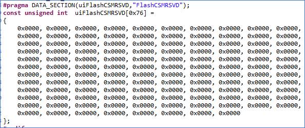
  1. Write 0x0000 to CSM_RSVD locations (starting from 0x3F7F80)


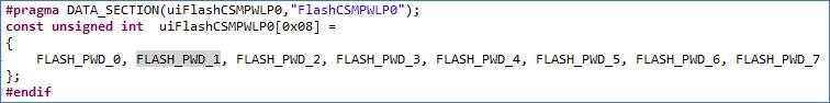
         2. Write PASSWORD (128-bit) to CSM_PWL_P0 locations (starting from 0x3F7FF8)


3. In the main() function, we “lock” the DSP by calling CsmLock() which is a function already defined in DSP2803x_SysCtrl.c.  If we want to debug, then we simply comment-out and not call CsmLock()

The info provided in SPRUI33C is quite detailed but unfortunately not very clear for me. 

Do you have a document that explains better the steps to enable security and also to disable it?  Maybe a code example will help.

I’m trying to be cautious here because I don’t want to lock the DSP and end up locking it forever.  We have a few board available but not a lot.

Regards Bernd

  • Hi,

    Since we have dual zone security on this device, the RAMs and Flash can be assigned to any zone. If you are only using one zone then you can allocate all the resources to one zone (please refer the TRM to see valid value to program) and program the passwords along with other settings. All the setting needs to be programmed in USER OTP. To start with you can use the flash plug-in GUI to program the settings.

    Unlocking the zone is same as previous device. You need to write the correct password value into KEYx register and zone will be unlocked.

    Regards,

    Vivek Singh

  • Vivek,

    datasheet sprs945d -> Table 6-3 shows:

    • DCSM_OTP_Bank0 starts at 0x78000 -> this OTP bank is for Flash Bank0 sectors?
    • DCSM_OTP_Bank1 starts at 0x78400 -> this OTP bank is for Flash Bank1 sectors?

     TRM SPRUI33C -> Table 3-17 shows:

    • Describes registers from 0x78010 to 0x783FA -> these are the blocks located in DCSM_OTP_Bank0?
    • For DCSM_OTP_Bank1, I don’t see any table describing the registers?

    You mentioned “All the setting needs to be programmed in USER OTP”… is there a code example for this?  SPRUI33C show an example for unlocking but not how to lock the MCU.

    We also would like to enable locking and set the password from within the binary code so that it is automatically enabled during first-time programming.  In our factory, we would like to keep the programming procedure simple to avoid mistakes.

    The F2803x examples I showed is a snippet of our actual code. Security is enabled and passwords are automatically written into the correct MCU locations when the MCU is programmed the first time.   

    SPRT731A did not discuss security, so I still don’t which exactly is the CSM_RSVD and CSM_PWL_P0 locations for Potenza.  I think it is one of the registers described in TRM Table 3-17 but I’m not sure.

    Can you comment.

    Regards Bernd

  • Hi Bernd,

    For DCSM_OTP_Bank1, I don’t see any table describing the registers?

    Table 3-17 shows the value programmed by TI for different fields in OTP BANK0. In OTP BANK1, none of the fields are programmed by TI. They have default values ALL_1 hence there is no mention of that.

    You mentioned “All the setting needs to be programmed in USER OTP”… is there a code example for this?  SPRUI33C show an example for unlocking but not how to lock the MCU.

    There is an DCSM example in C2000Ware (<C2000Ware>\driverlib\f28004x\examples\led). It is only sample asm and link cmd file which need to be included in main project and also the security settings need to be updated as per usecase.

    SPRT731A did not discuss security, so I still don’t which exactly is the CSM_RSVD and CSM_PWL_P0 locations for Potenza.  I think it is one of the registers described in TRM Table 3-17 but I’m not sure.

    All the security settings are in USER OTP (not register) which need to be programmed with different security settings. Passwords locations part of Zone Select block and address for Zone Select block can be changed by changing the link pointer so that if needed user can update some of the security settings (e.g. password value) in future.

    Regards,

    Vivek Singh