This thread has been locked.

If you have a related question, please click the "Ask a related question" button in the top right corner. The newly created question will be automatically linked to this question.

F28335 ADC shows incorrect values


Hi,
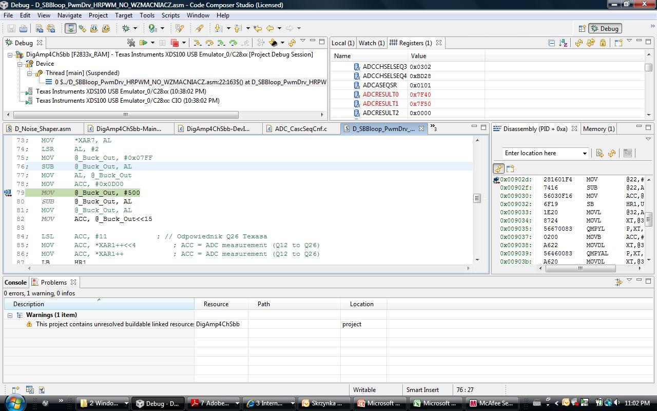
I'm working on power control application using F28335. I need to sample voltage on the B0 input pin. I put 0.3V which should give approx. 4096/10 =0x19A. But when I run my code in the debug mode it shows for the first a few debug stops between 0x7F1 and 0x7F5 and then these values interleaved with some divergent ones like 0x0500, 0x600, etc. I look up the values both in the ADCRESULTx and the buffer registers at 0x0B0x. Can the 50ms the ADC documentation's talking about needed after ADC power-up be a problem in the debug mode ?  Even is the B) pin was by mistake not connected can the ADC result registers show value that suggests ADC sees 1.5V on the input ? (0x7FF -> 1.5/3V)
Here is the code that I'm using for 16 cascaded conversions in the continuous mode:


void


ADC_CascSeqCNF(int ChSel[], int ACQPS, int NumConvSEQ1, int mode)
{
// ADC power-up sequence
AdcRegs.ADCTRL3.bit.ADCBGRFDN = 0x3;
// Power up bandgap/reference circuitry
AdcRegs.ADCTRL3.bit.ADCPWDN = 0x1;
// Power up rest of ADC
// ADC Acquisition window select and Channel allocation
AdcRegs.ADCTRL3.bit.ADCCLKPS=0;
// ADCCLK=12.5 MHz @ HSCLK=25MHz
AdcRegs.ADCTRL1.bit.ACQ_PS= ACQPS;
// Window aperture
// ADC Sequencer and Interrupt Init
AdcRegs.ADCTRL1.bit.SEQ_CASC = 1;
// Single 16 state sequencer
AdcRegs.ADCTRL1.bit.SEQ_OVRD = 0; // Wrap at MaxConv// # of Conversions & Input channel Allocation
AdcRegs.ADCMAXCONV.all = (NumConvSEQ1-1);
// Number of conversions
AdcRegs.ADCCHSELSEQ1.bit.CONV00=ChSel[0];
// 1st conv - Sequencer 1
AdcRegs.ADCCHSELSEQ1.bit.CONV01=ChSel[1]; // 2nd conv - Sequencer 1
AdcRegs.ADCCHSELSEQ1.bit.CONV02=ChSel[2];
// 3rd conv - Sequencer 1
AdcRegs.ADCCHSELSEQ1.bit.CONV03=ChSel[3];
// 4th conv - Sequencer 1
AdcRegs.ADCCHSELSEQ2.bit.CONV04=ChSel[4];
// 5th conv - Sequencer 1
AdcRegs.ADCCHSELSEQ2.bit.CONV05=ChSel[5];
// 6th conv - Sequencer 1
AdcRegs.ADCCHSELSEQ2.bit.CONV06=ChSel[6];
// 7th conv - Sequencer 1
AdcRegs.ADCCHSELSEQ2.bit.CONV07=ChSel[7];
// 8th conv - Sequencer 1
AdcRegs.ADCCHSELSEQ3.bit.CONV08=ChSel[8];
// 9th conv - Sequencer 1
AdcRegs.ADCCHSELSEQ3.bit.CONV09=ChSel[9];
// 10th conv - Sequencer 1
AdcRegs.ADCCHSELSEQ3.bit.CONV10=ChSel[10];
// 11th conv - Sequencer 1
AdcRegs.ADCCHSELSEQ3.bit.CONV11=ChSel[11];
// 12th conv - Sequencer 1
AdcRegs.ADCCHSELSEQ4.bit.CONV12=ChSel[12];
// 13th conv - Sequencer 1
AdcRegs.ADCCHSELSEQ4.bit.CONV13=ChSel[13];
// 14th conv - Sequencer 1
AdcRegs.ADCCHSELSEQ4.bit.CONV14=ChSel[14];
// 15th conv - Sequencer 1
AdcRegs.ADCCHSELSEQ4.bit.CONV15=ChSel[15];
// 16th conv - Sequencer 1
if (mode==0)
{AdcRegs.ADCTRL1.bit.CONT_RUN = 0;
// Start-Stop Conv mode
AdcRegs.ADCTRL2.bit.EPWM_SOCA_SEQ1 = 1; // Start Conv via ePWM SOCA trigger event}

if
(mode==1)
{AdcRegs.ADCTRL1.bit.CONT_RUN = 1;
// Continuous Conv mode
AdcRegs.ADCTRL2.bit.SOC_SEQ1 = 1;
// Kick-start the ADC now}}

It is called from the main() with the following code


for(i=0;i<16; i++) ChSel[i] = 8;


//void ADC_CascSeqCNF(int ChSel[], int ACQPS, int NumConvSEQ1, int mode)

ADC_CascSeqCNF(ChSel, 2, 16, 1); 

// ACQPS=2, #Conv=2, Mode=Continuous

}


  • Certainly you do need to add the power up delay to your code as spec'd in the DS after the ADC is turned on; but I do agree that if you are single stepping/breakpointing after this power up happens then you are most likely observing the required time. 

    I do not see where you have set the HSPCLK divider to get the ADC clock to 25MHz, this should be in your main as well but I want to make sure.  If ADC Clock >25MHz results will be unpredictable.  I'm assuming you are running the core @150MHz, so you will need a value of 3(which gives divider of 6) to get 25MHz.

    From code you are sampling ADCINB0, have you confirmed voltage at the pin?

    Best,

    Matthew

  • Hi Matthew,
    thank you for a quick reply. I added a delay loop:  for(i=0; i<1E+4; i++) for(i1=0; i1<5; i1++);
    checked the clock: SysCtrlRegs.HISPCP.all = 0x0003; and   SysCtrlRegs.PCLKCR0.bit.ADCENCLK = 1; // ADC

    and connected the ADCINB0 to the ground but it still consistently shows sth around half the max value. The ADC hardware is reacting to my setup as it shows just two conversions, as I specified. Hope you might have some more hints ...


  • Can you post/attach the contents of all ADC registers?  I just want to look at everything that is setup in case there is something I am missing.

    Along these lines; this device requires ADC calibration SW routine be ran before conversions, to properly trim the internal circuits to meet the DS. 

    1)Can you confirm this is done

    2)Can you confirm there is NOT a SW reset issued to the ADC regs(ADCTRL1 I think) after this is done?  Reason is that ADC Reset will clear out the trim registers and cause ADC to give bad results.  In this case ADC calibration would need to be re-called by the SW.  Data dump will tell me if these are in correct state or not.


    Best,

    Matthew


  • Thank you for this solid and attentive support. I have been silent for a while since in the meantime I have assembled another prototype PCB and it seems the hardware is at fault. The same software works OK for the new PCB. I also measured the resistance of the ADC inputs to the ground and on the new, working PCB all of them showed some hudrends Ohm but on the not-working old one out of four ADC inputs that are available on my PCB  (A0, A1, B0, B1)  three showed also 600-700 Ohm but one - B1 showed low resistance ca. 15 Ohm. However, it is not only the B1 input on the old one that is not working, I got the same 0x7F0 values when I applied ground and followed the other inputs. The uC on the old PCB does not show any other misbehaviour, processor and PWM-s work flawlessly.

    I would simply switch to the new PCB for testing and forget the old one but the problem is I have managed to burn the new one soon after the test and now I'm left with the old one with little possibility to replace either uC as f28335 is not available at the moment at any distributors in the world...
    Is it possible that the ADC section would be somehow broken while the rest OK ? Or there is a chance there is sth wrong with my PCB that makes the ADC section mulfunction - any way to check it somehow ?

    Best regards,

    Pawel

  • Pawel,

    I think that if one ADC channel is showing too low resistance then it also has the potential to disturb the other channels since they share a  mux with the ADC.   It sounds like there has been some damage to the analog portion of the device.  Is the current draw on the analog power domain within the DS limit?  If not it would be a clear indication some damage has occurred.

    Can you comment if the ADC channels are seeing a volage before the power is applied to the device?  Any voltage on the ADC inputs should be kept at or below the 3.3V power rail as it ramps up during power up.  In the same vein the 3.3V analog power should be ramped at the same time as the 3.3V digital supply.

    Additionally even while running the analog inputs must stay at or below VDDA level; which is 3.3V nominally.

    Please let me know your observations.

    Best regards,
    Matthew

  • I thinks I also encounterd some problems with ADC conversion, to much noise, for example, when I connected A0 channel to GND, of course, most of the time I saw the ADCRESULT0 show around 0x000, but sometimes it jump like a crazy horse, even to 0x1xxx! 

    Here's my ADC code:

    InitAdc();

    // Specific ADC setup for this example:

      AdcRegs.ADCTRL1.bit.ACQ_PS   = ADC_SHCLK;

      AdcRegs.ADCTRL3.bit.ADCCLKPS = ADC_CKPS;

      AdcRegs.ADCTRL1.bit.SEQ_CASC = 1;        // 1  Cascaded mode

      AdcRegs.ADCTRL1.bit.CONT_RUN = 0;       // Setup non-continuous run

      AdcRegs.ADCTRL1.bit.SEQ_OVRD = 0;       // Disable Sequencer override feature

      AdcRegs.ADCMAXCONV.bit.MAX_CONV1 = 0x0001; // Setup 2 conv's on SEQ1

      AdcRegs.ADCCHSELSEQ1.bit.CONV00 = 0x0; // Setup ADCINA0 as 1st SEQ1

      AdcRegs.ADCCHSELSEQ1.bit.CONV01 = 0x1; // Setup ADCINA1 as 2nd SEQ1

    while(1)

    {

    delay_ms(1);    //delay 1ms

    AdcRegs.ADCTRL2.bit.RST_SEQ1 = 1;       // Reset SEQ1

    AdcRegs.ADCTRL2.bit.SOC_SEQ1 = 1; // Start ADC conversion

    AdcRegs.ADCTRL2.bit.INT_ENA_SEQ1 = 1;  // Enable SEQ1 interrupt (every EOS)

    }

    interrupt void  adc_isr(void)

    {

    Vd1_new= AdcRegs.ADCRESULT0 >>4;

    Vd2_new= AdcRegs.ADCRESULT1 >>4;

       AdcRegs.ADCST.bit.INT_SEQ1_CLR = 1;       // Clear INT SEQ1 bit

    AdcRegs.ADCTRL2.bit.INT_ENA_SEQ1 = 0;  // Disable SEQ1 interrupt 

       PieCtrlRegs.PIEACK.all = PIEACK_GROUP1;   // Acknowledge interrupt to PIE

      return;

    }


    Please give me some advices!

  • Duy, please start a new thread for your issue.  Thanks.