This thread has been locked.

If you have a related question, please click the "Ask a related question" button in the top right corner. The newly created question will be automatically linked to this question.

TMS320F280049: Digital peripheral module glitch

Part Number: TMS320F280049

Greeting,

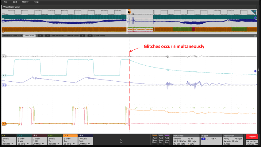
I am using F280049 for three phase PFC control, the problem occurred occasionally that EPWM and GPIO outputs is forced high, low, or high impedance. As shown the following scopes, Ch1 is the clock that I use Timer1 of 1ms to toggle GPIO7, Ch2 is a debug EPWM output does not connect the driver circuit and set 50% duty, Ch3-Ch5 are EPWM outputs to connect the driver circuit, Ch6 is a phase current for triggering scope.

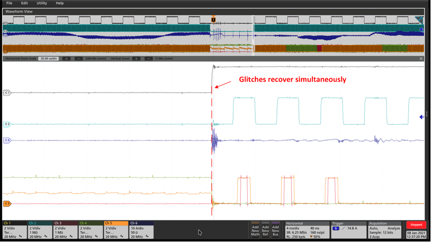
I found all GPIO and EPWM glitches appear and recover simultaneously. Besides, CPU and analog modules are running because duty cycles of EPWM outputs are correct after recovery.

I also capture another scope shows DAC and ADC are running normally when the glitch occurred as below. Ch1 is a debug GPIO output triggered by 20us ISR run time, Ch2 is another debug GPIO output triggered by 1ms ISR run time, Ch3 is buffered DACA to output the ADC sampling of one phase voltage and updated in 1ms ISR, Ch4 is buffered DACB to output ADC sampling of another phase voltage and updated in 20us ISR. The scope shows ADC, DAC, and CPU are work normally when GPIO glitch occurred.

What will cause the digital peripheral module glitch like this? Any suggestions to avoid this issue?

Regards,

Watch

  • Hi Watch,

    Thanks for your detailed waveforms and explanations. Do you have any code that will force the CH1 GPIO to be low?

    I just want to first exclude the condition that any potential unused code triggers the glitches.

    Regards,

    Chen 

  • Hi Chen,

    The Ch1 GPIO is using below codes to toggle the high/low state in CPU_Timer1_ISR of 1ms:

    This statement is asserted in CPU_Timer1_ISR only.

    Besides, the GPIO is configured and cleared before running applications. However, the glitch doesn't cause MCU reset because ADC, DAC, and CPU are running normally when the glitch occurred.

    Regards,

    Watch

  • Hi Watch,

    Have you measured the CPU bandwidth of each ISR?  I am thinking whether it is because of the CPU is fully occupied under certain condition that the low priority ISR got delayed.

    Regards,

    Chen

  • Hi Chen,

    Thank you for your reply.

    I have checked the CPU usage does not exceed 100% when the glitch occurred. I use two nested ISRs of CPU for this project, one is the lower priority ISR of 1ms CPU_Timer1, the other is the higher priority ISR of 20us ADC_EOC. As shown the following scope, Ch2 is buffered DACA to output the percentage of run time triggered by the 1ms ISR, Ch5 is buffered DACB to output the percentage of run time triggered by the 20us ISR, Ch3 is a debug EPWM output does not connect the driver circuit and set 50% duty, Ch6 is a phase current for triggering scope.

    The result is matched as the scope I mentioned which shows CPU, ADC, and DAC are working normally when the glitch occurred.

    Regards,

    Watch

  • Hi Watch,

    Thanks for your update. Let me check it on my side and will get back to you tomorrow.

    Regards,

    Chen

  • Is everything else in the device operating as expected when the glitch occurs? The surrounding GPIOs?

    Nima

  • Watch, 

    I believe we have closed this off-line, but I wanted to come back here and document my understanding since it is an interesting case.

     We suspect that the IO’s on the device were going tri-state or drive-high/low due to an unwanted entry into IEEE 1149 JTAG Boundary Scan mode.  This device does not have an nTRST pin so it is possible that occasional noise transitions on TCK and TMS could accumulate over time and advance the JTAG state machine to a boundary scan mode which has this effect.

     The direct way to avoid this issue is to ensure TCK and TMS are noise-free during operation (placed far away from noisy signals) and have sufficiently strong pull-up resistors to keep them in a known state.

     As a debug method, the TAP_STATUS register will indicate the current state of the JTAG state machine.  Normally when the debugger is dis-connected (DCON=0) the TAP_STATE should be 0x0 or Test Logic Reset.  It is possible other values may be in this register based on power up sequences of TMS and TCK as well, but it should not be changing over time.  If TAP_STATE is changing, that is an indication of TMS-TCK transitions.  The debugger will also initiate changes to the TAP_STATE  when connecting and before DCON=1, so some delay in debug code may be needed when reading DCON status to determine if any TAP_STATE change is due to the debugger connecting (expected) or due to board noise (undesired).

     There is a one-shot (temporary) reset register SOFTPRES40 which issues an internal nTRST pulse to reset JTAG.  This register is currently not documented but will be added in the next TRM revision.

    Best regards,

    Jason

  • Hi Jason,

    I agree with your suspicion that an unwanted JTAG activity causes unexpected IO states. In fact, this issue doesn't appear after we have redesigned the PCB to place JTAG signals far away the PFC output.

    Regarding the debugger connection, I have inserted a debug code into my project to check TAP_STATE changes when the debugger connecting. The result is consistent with your mention that there shall have some delay before reading DCON status for verifying JTAG state.

    Can you provide the specified value of the delay time?

    Regards,
    Watch

  • Watch,

    The delay time is difficult to determine.  This will depend on the PC sending commands to the debugger, the debugger used, TCK frequency, as well as the asynchronous time interval between the F28004x device coming out of reset and a debugger attempting to connect. 

    As long as the debugger would be connected on a power-up condition, then this delay to check DCON can be done only one time on device initialization.

    Best regards,

    Jason