This thread has been locked.

If you have a related question, please click the "Ask a related question" button in the top right corner. The newly created question will be automatically linked to this question.

TMS320F28335: Using McBSP as SPI operation

Part Number: TMS320F28335

Dear Champs,


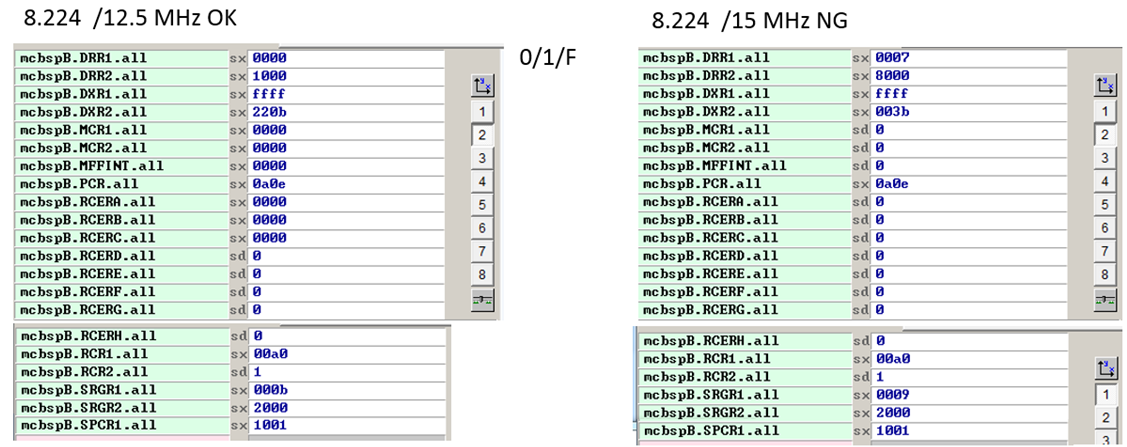
We used McBSP as SPI operation by using clock stop mode on F28335. According the register values we set, mcbspB.SPCR1.all= 0x1001h, it means bit12-11 is 10 for clock stop mode without clock delay. It means the clock starts immediately (CLKSTP = 10b) at the beginning of each data transfer.

But we found it still need to add 2bit data delay on RCR2 for correct communication when CLKR is 15MHz.
There is a confusion for RDATDLY, “A data delay value of 0 or 2 is undefined in the clock stop mode”.
Does anyone know what is this contradiction?

If you have any suggestions, please feel free to let me know.

Thanks a lot.

Best regards,

Janet

  • Janet,

    From your description of RDATDLY, I assume the customer is using our McBSP as the SPI Master; could you also advise on the state of the CLKXP and CLKRP bits?  I want to make sure I have correct understanding of the expected timings like page 695 of the TRM.  

    Also on page 696, can we confirm that customer code is following the procedure from releasing from reset?  Specifically the 2 sample rate generator clock wait after bringing sample rate generator out of reset, as well as when we release the transmitter and receiver from reset.

    I'm not sure what value of 2 in RDATDLY would do in this mode since it mentions it is undefined.  Is the customer seeing this have different behavior than value of 1?

    Best,

    Matthew

  • Matthew,

    1.I checked the our code is following all  the procedure of user manual.

    2 I use the same code and  setup the the communication rate to be 12.5M Hz. No matter  1 or 2 in RDATDLY , there is no different behavior. It all works normally.

      I check the setup time of MISO signal is great than 30ns. 

      As long as I setup the the communication rate above the 15M Hz, I have to set 2 in RDATDLY to make communication functional because I notice that setup time of MISO signal is 22ns.

  • Changhuan,

    Thank you for the extra detail, can you share all the McBSP register settings for both 12.5MHz and 15MHz operation?  Can you also share the LSPCLK divider info?  If it is easier to just get a screen shot of the register in CCS that will be fine.

    I want to be sure I understand the clock rates at the McBSP boundary as well as in the clock generation circuitry.

    Please also confirm the CPU clock, is it 150MHz?

    The behavior of RDATDLY at 12.5MHz(i.e. no difference if 1 or 2) is what I would normally expect.

    Best,
    Matthew

  • All the register setup as below

    "OK" means the receive data is correct.

    I confirm the CPU clock is 150MHz.

  • Changhuan,

    Thank you for the information.  I'd like to try the following:

    Based on the value of CLKGDV in SRGR1 register, I believe that your low speed clock divider is 1(LOSPCP = 0).

    I'd like to change LOSPCP = 1, which would make the low speed clock = 150/2 = 75MHz.

    Then change CLKGDV to values of 5(for 12.5MHz) and 4(for 15MHz) and see if the SPI  mode works correctly with this change in clocks.

    Best,

    Matthew

  • Mattew

    I followed your suggestion and tested by set  CLKGDV to values of 5(for 12.5MHz) and 4(for 15MHz). All results are not okay.

    When I set CLKGDV to values of 9( for  7.5MHz), the SPI mode works correctly.

  • Changhuan,

    Can you clarify if the C28x is the SPI Master or Slave?  From the clock limitations it appears we are in slave mode, there is a slave clock min divider of 8 LSPCLKs due to how the McBSP samples the incoming clock.

    Best,

    Matthew

  • Matthew,

    According to the registers table that I attached,I set up McBSP as SPI Master in my design. I know the limitations in the slave mode. However, there is no information about SPI master. For example, the maximum frequency for my application requirement. Could you help me calculate?

    I made a test and found an interesting thing that the communication worked (shown in below) even setup time could be small than 30ns. According to the SPI timing constraint, it should have some  problem. 

    Do you think the  McBSP as SPI Master setup Timing Requirements minimum is 30ns. Is the value correct? 

    yellow channel: CLK  (15M Hz)

    green channel:MISO

  • Changhuan,

    The max speed on this device is limited by the GPIO slew rate.  In this case that is capped at 25MHz across all conditions of the device; but it is not a binary type limit.  That is there may be some devices, and especially at nominal conditions(like room temperature and supply rail > Vmin) that will be able to give better performance as you saw on your device.

    I believe this is also a specification where you could also see a faster toggle rate, but the pin won't be able to transition correctly to is VOL/VOH spec the faster we go.  Let me know if you agree with the above explanation.

    At any rate, I think I may know the source of our issue on the receive; and it is the qualification logic that is inline on the GPIO pin itself.  The default setting is to synchronize the incoming signal with SYSCLK.  The issue is that this logic also exists inside the McBSP so we are syncing twice, causing delay in the Rx signal relative to the SPICLK.

    For whichever GPIO you have configured as the RX, you will want to change its GPAQSEL(or GPBQSEL) to ASYNC = 3(it will be set to 0 by default). 

    Let me know if this fixes the issue.

    Best,

    Matthew

  • Matthew,

    According to my test result, I think the max speed on this device is not only limited by the GPIO slew rate.   The issue is that this logic also exists inside the McBSP so you are syncing twice, causing delay in the Rx signal relative to the SPICLK. Does it means the max speed should be under 12.5MHz?

    For the GPIO23 I configured as the RX,   its GPAQSEL2 has been to be ASYNC = 3 in my current design. Therefore, we did not fix the issue.

  • Changhuan,

    I'm looking into this; I'll need another day to consult with some other C2000 team members.  As long as we are removing the sync at the GPIO there shouldn't be another synchronizer to CPU clock in the path.

    Could you confirm that the GPIO used for SPICLK is also set to ASYNC, even though this is an output?  While I don't think in SPI Master mode that the return path would be used to clock the internal logic, I'd like to rule that out as a potential issue.

    Best,

    Matthew

  • Matthew,

    I made a mistake and I would like to correct  previous information that I rely. 

    For the GPIO13 I configured as the RX,   its bits(27,26) of GPAQSEL1  are set to be 0

    For the GPIO14 I configured as the CLK,   its bit(29,28) of GPAQSEL1 are set to be 0

    After I set all of them to be ASYNC = 3, the communication works and the issue seems to be fixed.

    Would you please tell me the related information?

  • Changhuan,

    Thanks for the clarification on the setup, and glad things are working as documented.

    Since the McBSP in SPI mode is relying on relative timings to its own SPICLK, I believe that the default synchronizers on the GPIOs could introduce propagation delay since they won't pass the incoming data until 1 CPU clock has passed. 

    Since the SPI protocol relies on the incoming data to be latched on the falling edge of the SPICLK this will push the data out as we use SPI clocks closer to the CPU clock rate.

    I also want to correct an earlier statement on the max speed of the McBSP in SPI mode.  I had mentioned that we should be able to operate at 25MHz SPI Clock, based on the GPIO limitation. 

    Janet had pointed out that there is a 30ns setup time requirement on DX(receive) data before the falling SPI Clock.  This isn't possible at 25MHz(40ns period or 20ns half period).  This would cap full duplex SPI at 16.6MHz, while half duplex transmit could run at 25MHz. 

    Your data rate of 15MHz clock is still within this range, so we can realize full duplex at your needed speed.

    The native SPI module on this device is capable of 25MHz full duplex, which is where the confusion came on my end.

    Best,

    Matthew