This thread has been locked.

If you have a related question, please click the "Ask a related question" button in the top right corner. The newly created question will be automatically linked to this question.

LAUNCHXL-F28027F: F28027F I2C not working

Part Number: LAUNCHXL-F28027F
Other Parts Discussed in Thread: DRV8301, MOTORWARE

Hi

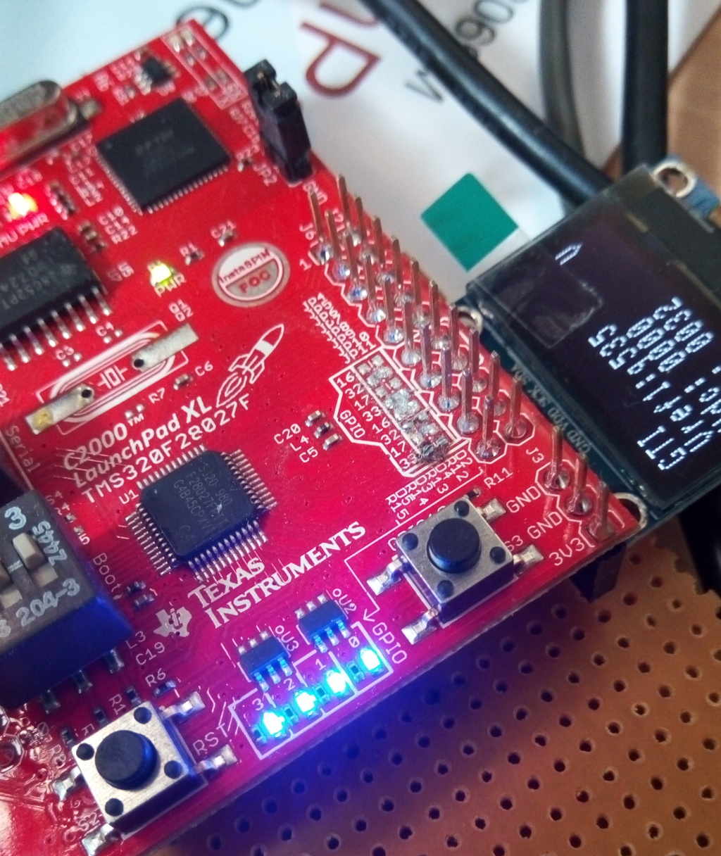
I adapted a program that displays on OLED screen with launchpad F28069M to F28027F launchpad

   // 90 MHz/( (8+1)(10+5 + 5+5)) = 400 kHz

   // 60 MHz/( (5+1)(10+5 + 5+5)) = 400 kHz

   I2caRegs.I2CPSC.all = 5;                         // Prescaler - need 7-12 Mhz on module clk

   I2caRegs.I2CCLKL = 10;                             // NOTE: must be non zero

   I2caRegs.I2CCLKH = 5;                              // NOTE: must be non zero

but on the I2C EEPROM example of F28027F they say we have to put

   I2caRegs.I2CPSC.all = 6;

this will not give the 400 kHz ?

also I have no signal at all on I2C

Though I have configured I2C pins and shorted the JP9 and JP11

// I2C used on GPIO32/33   LB 04/2018 F28027F
  // il faut souder JP9 et JP11
  // I2C Data
  GPIO_setMode(obj->gpioHandle,GPIO_Number_32,GPIO_32_Mode_SDAA);
  // I2C Clock
  GPIO_setMode(obj->gpioHandle,GPIO_Number_33,GPIO_33_Mode_SCLA);
  // config I2C
  GPIO_setPullup(obj->gpioHandle,GPIO_Number_32, GPIO_PullUp_Enable);	// Enable pull-up for GPIO32 (SDAA)
  GPIO_setPullup(obj->gpioHandle,GPIO_Number_33, GPIO_PullUp_Enable);
  GPIO_setQualification(obj->gpioHandle,GPIO_Number_32, GPIO_Qual_ASync);// Asynch input GPIO32 (SDAA)
  GPIO_setQualification(obj->gpioHandle,GPIO_Number_33, GPIO_Qual_ASync);

  • Lofti,

    Based on the timings of the example, you are correct that it is not set up to communicate at 400 kHz. I will file a ticket to update the example, but cannot guarantee when it will be fixed. The examples are meant to be a starting point. The I2C protocol is set up to handle up to 400kHz clocks. As long as the I2C prescaled clock is within 7-12 MHz, the module will guarantee that the timings can be met. You can adjust the I2CCLKH and I2CCLKL registers to provide additional width in each of these regions. Alternately, just change I2CPSC to 5, and you will have 400 kHz exactly.

    Please check that the I2C peripheral clock is enabled.

    Please tell me if you have done any other modification to the LP. The pads that you have shorted on JP9 and JP11 are actually already shorted through a trace that runs beneath the pad. You can see this in the schematic. Have you connected anything to J2.6 and J2.7? If so, have you cut the trace between JP5 and JP7?

    Thanks,
    Mark
  • Hi Marks,

    I don't see any trace between pads, just small amount of soldering for a 0603 R0 on the pads.

    Are you sure there is a link ? How can I cut them

    I want (not done yet) to connect an EVM8301 so it will use the SPI on J2.6 and 7 so I need to solder JP4 and JP6 (not done yet)

    J2.6 SDI JP4-ON

    J2.7 SDO JP6-ON

    and to connect OLED using I2C on 

    J6.7 GPIO32 SDA_OLED JP9-ON

    J6.8 GPIO33 SCL_OLED JP11-ON

    So I soldered JP9 and JP11

    My program dosen't work... though it was working on 69M so it is for sure the config / hardware

    --------------------------------------------

    I imported  Example_2802xI2C_eeprom.c  (after having modified GPIO so that 

    GpioCtrlRegs.GPBMUX1.bit.GPIO32 = 1; // Configure GPIO32 for SDAA
    GpioCtrlRegs.GPBMUX1.bit.GPIO33 = 1; // Configure GPIO33 for SCLA

    The example  Example_2802xI2C_eeprom.c  works ! I got signals out from the

    I2C J6.7 J6.8

    So what's wrong with my program

    how to check "Please check that the I2C peripheral clock is enabled."?

    Yes the solution where there !

    By default the 

    void HAL_setupPeripheralClks(HAL_Handle handle)

    has

    CLK_disableI2cClock(obj->clkHandle);

    whereas for F28069M it enables I2C!

    but my prog still doesn't work

    it still get stuck  while waiting for .I2CSTR.bit.XRDY

    for (i=0; i<wsize; i++)
    {
    I2caRegs.I2CDXR = *(wdata+i);
    while(!I2caRegs.I2CSTR.bit.XRDY);
    }

    any idea?

    thanks

  • Lotfi,

    The trace is there in between the pads. It is buried. You can tell this by measuring the the resistance between the pads or checking the continuity with a DMM. You can cut the trace with an exacto knife. It is buried just below the soldermask so you do not need to slice very deep. This was a very early LaunchPad before a full ecosystem specification had been finalized, as well as it using a low pincount package, so some tradeoffs were made to get as many pins as possible where they could logically go.

    For your hardware configuration, please set up the jumpers as follows

    BP pin Signal Desired Connect Cut
    J2.6 GPIO - SDI JP4 JP5
    J2.7 GPIO  - SDO JP6 JP7
    J6.7 GPIO32 - SDA JP9 JP8
    J6.8 GPIO33 - SCL JP11 JP10

    Now your hardware should be set up to accept both boards without contention.

    I am a bit confused on which program you are using. You have stated that you are adapting your OLED driver code written for F2806x (linked here https://github.com/blotfi/c2000_OLED_SSD1306) and that you are attempting to add the DRV8301 BoosterPack. Are you now working one of these labs: C:\ti\motorware\motorware_1_01_00_18\sw\solutions\instaspin_foc\src ? If so, yes, the code disables the I2C module, likely to reduce power consumption and also because it is not necessary in the program example.

    Did you change the line 

    Lotfi said:
    CLK_disableI2cClock(obj->clkHandle);

    to 

    CLK_enableI2cClock()?

    -Mark

  • Thank a lot Mark

    Yes I already enabled I2C clk   CLK_enableI2cClock in my modified HAL.c file

    but your last post solved the issue definitively when you explain me that the traces are buried!

    Yes when testing all connections where ON !

    Couldn't cut them with a scalpel, si I went with my Dremel 0.8 mm ;-) works fine

    Now my pb is solved: PWM with its 8301 over SPI and OLED screen I2C work

    (yes  https://github.com/blotfi/c2000_OLED_SSD1306 is my code for 69M and works for 27F now also)

    your table  should be printed in the Launchpad 27F schematics or user's guide

    BP pin Signal Desired Connect Cut

    J2.6 GPIO - SDI JP4 JP5

    J2.7 GPIO  - SDO JP6 JP7

    J6.7 GPIO32 - SDA JP9 JP8

    J6.8 GPIO33 - SCL JP11 JP10

  • I am glad that the connections were the issue. I'll submit a ticket to get the table documented in the User Guide.

    -Mark

  • Hi Mark

    Yes it was an "underground jumper" issue.

    now I am dealing with an ADC ISR that is too long and that cuts the main loop (background task) that sends over I2C, info to be displayed on the OLED

    It is a pity to have only 4 level FIFO for I2C TX.

    A DMA with plenty of memory access would be much better.

    I am trying to find a solution for that, perhaps cut by small character parts or perhaps going into I2C TX ISR, but this is another story.

    All the best

    Lotfi