This thread has been locked.

If you have a related question, please click the "Ask a related question" button in the top right corner. The newly created question will be automatically linked to this question.

MSP430F5172: MSP430F5172 - Using DMA for ADC reading

Part Number: MSP430F5172

Hello, 

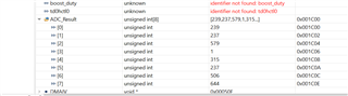
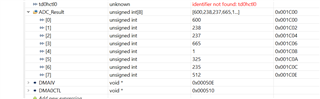
I am programming MSP430f5172 microcontroller. I have 3 voltage and 3 current sensors in my power converter. I am planning on using a DMA channel for storing ADC readings. I am able to get readings using my code but my initial thought was that if I declare an array for storing the data, it's value would correspond to each ADC channel and not change during each sensing but that's not the case, which means my sensor readings will get mixed up

I am new to this microcontroller and using DMAs. What am I doing wrong? Is it not possible to store the signal readings at a fixed array location?

Thank you

  • Hi Firehiwot,

    Let me look into this for you.

  • Yes, the goal is to have the buffer words correspond to each sample channel in order, but you have to configure the DMA appropriately. Can you post (or attach) how you're configuring the ADC and the DMA?

    I see a couple of ADC+DMA examples in Resource Explorer:

    msp430f51x2_adc10_10.c:

    https://dev.ti.com/tirex/explore/node?node=ACxR2ViLR-3U9df34vpizQ__IOGqZri__LATEST

    and msp430f51x2_adc10_14.c

    https://dev.ti.com/tirex/explore/node?node=AA0J2gkmfVYDIlaMkeFW7A__IOGqZri__LATEST

  • Hello, 

    thank you. Below is my code. I tried using example 10 and also used the configuration in the while loop from example 12, but I still have the same issue. 

    #include <msp430.h>
    #include <stdint.h>
    #include <math.h>

    //define functions
    void SetADC ();
    void SetDMA();
    unsigned int ADC_Result[8]; // 10-bit ADC conversion result array

    void main(void) {
    unsigned int i; // Declare counter variable
    volatile unsigned int D_buck; // buck duty cycle
    volatile unsigned int D_boost; // boost duty cycle
    volatile unsigned int bat_State; // battery switch state

    WDTCTL = WDTPW + WDTHOLD; // Stop watchdog timer

    // configure analog registers
    PMAPPWD = 0x02D52; // Enable Write-access to modify port mapping registers
    PMAPCTL = PMAPRECFG; // Allow reconfiguration during runtime
    P1MAP0|= PM_ANALOG; // Modify all PxMAPy registers - A0
    P1MAP1|= PM_ANALOG; // Modify all PxMAPy registers - A1
    P1MAP2|= PM_ANALOG; // Modify all PxMAPy registers - A2
    P1MAP3|= PM_ANALOG; // Modify all PxMAPy registers - A3
    P1MAP4|= PM_ANALOG; // Modify all PxMAPy registers - A4
    P1MAP5|= PM_ANALOG; // Modify all PxMAPy registers - A5
    P3MAP5|= PM_ANALOG; // Modify all PxMAPy registers - A8
    P3MAP6|= PM_ANALOG; // Modify all PxMAPy registers - A7
    PMAPPWD = 0; // Disable Write-Access to modify port mapping registers by writing incorrect key
    P1SEL|=BIT0+BIT1+BIT2+BIT3+BIT4+BIT5+BIT7+BIT8; // setting the port mapping register PxMAPy to PM_ANALOG together with PxSEL.y=1 when applying analog signals

    SetADC();
    SetDMA();

    while(1)
    {
    for(i=0;i<8;i++)
    {
    __data20_write_long((uintptr_t) &DMA0DA,(uintptr_t) &ADC_Result[i]); // Update destination array address
    while (ADC10CTL1 & BUSY); // Wait if ADC10 core is active
    ADC10CTL0 |= ADC10ENC + ADC10SC; // Sampling and conversion ready
    __bis_SR_register(CPUOFF + GIE); // LPM0, ADC10_ISR will force exit
    }

    __delay_cycles(5000); // Delay between sequence convs
    __no_operation(); // BREAKPOINT; check ADC_Result
    }

    }
    /*


    // DMA ISR
    #if defined(__TI_COMPILER_VERSION__) || defined(__IAR_SYSTEMS_ICC__)
    #pragma vector=DMA_VECTOR
    __interrupt void DMA0_ISR (void)
    #elif defined(__GNUC__)
    void __attribute__ ((interrupt(DMA_VECTOR))) DMA0_ISR (void)
    #else
    #error Compiler not supported!
    #endif
    {
    switch(__even_in_range(DMAIV,16))
    {
    case 0: break; // No interrupt
    case 2:
    // sequence of conversions complete
    ADC10CTL0 &= ~ADC10ENC; // Disable ADC conversion
    __bic_SR_register_on_exit(CPUOFF); // exit LPM
    break; // DMA0IFG
    case 4: break; // DMA1IFG
    case 6: break; // DMA2IFG
    case 8: break; // Reserved
    case 10: break; // Reserved
    case 12: break; // Reserved
    case 14: break; // Reserved
    case 16: break; // Reserved
    default: break;
    }

    // Configure ADC Channels
    void SetADC (){
    ADC10CTL0 = ADC10SHT_2 + ADC10MSC + ADC10ON; // 16xADC clock cycles, multiple sample conversion, ADC10ON
    ADC10CTL1 = ADC10SHP+ ADC10CONSEQ_1; // ADCCLK = MODOSC; sampling SIGNAL is sourced from the sampling timer, single seq.
    ADC10CTL2 = ADC10RES; // 10-bit conversion results
    ADC10MCTL0= ADC10INCH_8 + ADC10SREF_1; //Select ADC channel; USE VR+ = VREF and VR- = AVSS

    // By default, REFMSTR=1 => REFCTL is used to configure the internal reference
    while(REFCTL0 & REFGENBUSY); // If ref generator busy, WAIT
    REFCTL0 |= REFVSEL_2 + REFON; // Select internal ref = 2.5V
    __delay_cycles (75); // Delay (~75us) for Ref to settle -ADC10 sample & convert = (32+13)*2/SMCLK = 90/SMCLK = 75us

    }

    void SetDMA(){
    // Configure DMA0 (ADC10IFG trigger)
    DMACTL0 = DMA0TSEL_24; // ADC10IFG trigger
    __data20_write_long((uintptr_t) &DMA0SA,(uintptr_t) &ADC10MEM0); // Source single address
    DMA0SZ = 0x08; // 8 conversions - number of byte or word transfer
    DMA0CTL = DMADT_4 + DMADSTINCR_3 + DMAEN + DMAIE; // Rpt, inc dest, byte access, enable int after seq of convs
    }

  • > __data20_write_long((uintptr_t) &DMA0DA,(uintptr_t) &ADC_Result[i]); // Update destination array address

    With CONSEQ=1 and MSC=1, you'll get a burst (all 8 channels) for each loop (ADC10SC=1 setting), so you want the next loop to store in the same positions. Try:

    > __data20_write_long((uintptr_t) &DMA0DA,(uintptr_t) &ADC_Result[0]); // Set destination array base address

    Since this just sets the same value each time you can just do this once before the while(1) loop.

    [Edit: I just noticed this:

    > ADC10MCTL0= ADC10INCH_8 + ADC10SREF_1; //Select ADC channel; USE VR+ = VREF and VR- = AVSS

    The ADC10 samples from INCH to 0, so 8->0 is 9 channels. Try:

    > ADC10MCTL0= ADC10INCH_7 + ADC10SREF_1; //Select ADC channel; USE VR+ = VREF and VR- = AVSS

    ]

  • I have tried including this line of code in the setDMA() routine, without the for loop in the while (1) loop before, however I still have the same issue. I have included a picture below of the result that I have from the expressions table. I also thought this is how it is supposed to work since it is auto scanning all adc channels and will transfer data to the DMA during each iteration, but I am not getting the right output. 

  • In this test, I am only giving input to ADC channels 0, 1 and 4 and the correct ADC value should be ~240 

  • Thank you very much, changing it to ADC10INCH_7 made it work upto input channel 7. However, I am having issue with sending input channel 8. Since MSP430F5172 doesn't have A6 channel,  I thought the correct way to configure it would be to start from ADC10INCH_8 but make the size of the array 8 (since A6 is not sensed).

    I tried setting the array size to 9 and starting from ADC10INCH_8 but this didn't work. 

    How can I sense A8 if I configure it this way?

  • With the ADC10 there's no mechanism for skipping a channel in the sequence. [Ref User Guide (SLAU208Q) Fig 27-7]You have to go ahead and sample it, then ignore the result. You can even use the skipped channel for digital I/O -- the small sip of current the ADC takes during the sampling phase won't disturb anything.

    The alternative would be to convert single channels (CONSEQ=0) and change INCH in between, but that's usually more trouble than it's worth.

  • I see, I figured out the issue with my code. I would need to convert the DMA size to 9 as well in order to read A8. It's working now. Thank you very much. 

**Attention** This is a public forum