This thread has been locked.

If you have a related question, please click the "Ask a related question" button in the top right corner. The newly created question will be automatically linked to this question.

MSP430FG4618: Cannot flash device with CCS or MSPFlasher: Verification failed: Values at address 0x00010 do not match

Part Number: MSP430FG4618
Other Parts Discussed in Thread: TI-CGT

Hi,

I'm trying to compile and flash some legacy code onto the corresponding legacy hardware based on the MSP430FG4618 for a further development project.

First I imported the legacy code into Code Composer Studio 10.3.1.00003 and compiled with TI-CGT 21.6.0 LTS. The build succeeded, but when I tried to flash the device, I got a data verification error:

MSP430: File Loader: Verification failed: Values at address 0x00010 do not match Please verify target memory and memory map.

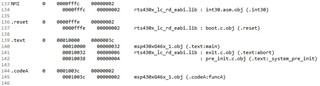
According to the data sheets, 010h is the memory address of the P3REN register.

I haven't modified the linker script that CCS generated, and I verified that the address 010h was mapped correctly.

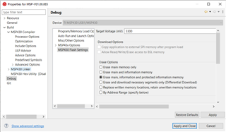
I also tried selecting the option to erase the main, information and protected information memory regions, but this didn't change anything.

When I try to flash another (small) program that I wrote from scratch to test the device (blink some LEDs, etc.), flashing and debugging work without problems.

Before I flashed the device, I had dumped the memory of the device with MSPFlasher into three files: main.txt (MAIN), info.txt (INFO), bootloader.txt (BSL):

C:\> MSP430Flasher -n MSP430FG4618 -r [main.txt,MAIN]
C:\> MSP430Flasher -n MSP430FG4618 -r [info.txt,INFO]
C:\> MSP430Flasher -n MSP430FG4618 -r [bootloader.txt,BSL]

When I tried to recover the old firmware with the following commands:

C:\> MSP430Flasher -n MSP430FG4618 -w main.txt -v -z [VCC=3300, RESET]
C:\> MSP430Flasher -n MSP430FG4618 -w info.txt -v -z [VCC=3300, RESET]
C:\> MSP430Flasher -n MSP430FG4618 -w bootloader.txt -v -z [VCC=3300, RESET]

main.txt succeeds, but info.txt and bootloader.txt fail with the same error:

* -----/|-------------------------------------------------------------------- *
*     / |__                                                                   *
*    /_   /   MSP Flasher v1.3.20                                             *
*      | /                                                                    *
* -----|/-------------------------------------------------------------------- *
*
* Evaluating triggers...done
* Checking for available FET debuggers:
* Found USB FET @ COM14 <- Selected
* Initializing interface @ COM14...done
* Checking firmware compatibility:
* FET firmware is up to date.
* Reading FW version...done
* Setting VCC to 3300 mV...done
* Accessing device...done
* Reading device information...done
* Loading file into device...
# Exit: 59
# ERROR: Could not write device memory
* Starting target code execution...done
* Disconnecting from device...done
*
* ----------------------------------------------------------------------------
* Driver      : closed (No error)
* ----------------------------------------------------------------------------
*/

What could be cause of these problems? How can I further investigate it?

Thank you in advance.

  • Hello,

    The following thread is similar and may help you resolve your issue.

    CCS/MSP430FG4618: File Loader: Verification failed when adding BSL as in slaa600d

  • Hi,

    I had a look at the forum thread you referenced and tried the following:

    1. Delete the debug configuration as explained here.
    2. Delete the .metadata folder in my workspace and reimport the project into CCS.
    3. Create a new workspace.
    4. Delete the following folders from the project folder:
      • .launches
      • .settings
      • Debug
      • targetConfigs
    5. Delete the aforementioned folders, delete the linker script lnk_msp430fg4618.cmd, delete the project from the workspace and reimport it.
    6. Delete all the aforementioned files plus the following files, and then create a new workspace and create a new project in the folder of the existing source code:
      • .ccsproject
      • .cproject
      • .project

    None of this helped. I still get the very same error message:

    MSP430: File Loader: Verification failed: Values at address 0x00010 do not match Please verify target memory and memory map.

    In addition, I tried to program both a production version of our old custom hardware and an MSP-EXP430FG4618 board, and I get the same error with both, which tells me that the hardware is not the problem, but something in the software or how it's being built.

    The error message says that I should verify the target memory and the memory map.

    I was able to find a .map file in the Debug folder.

    I had a look at it, and it seems that one of our functions is being place at a custom code section named CODE_UPLD with the #pragma codeseg (of our previous compiler), which we changed to #pragma CODE_SECTION for TI-CGT.

    Apparently, this section is not mapped in the default linker script, and for some reason the linker is mapping it to address 00000010 in the map file:

    SECTION ALLOCATION MAP
    
     output                                  attributes/
    section   page    origin      length       input sections
    --------  ----  ----------  ----------   ----------------
    CODE_UPLD 
    *          0    00000010    000000d0

    I'm still confused about this, though, because the memory mapping of the 8-bit peripheral registers should correspond to RAM, but the code sections should be stored in the flash, so P3REN should be mapped to RAM address 0x10, and this function should be at address 0x10 of the flash, and these address spaces should be independent, right?

    Here's the content of the linker script that CCS created, which I didn't modify at all:

    /****************************************************************************/
    /* Specify the system memory map                                            */
    /****************************************************************************/
    
    MEMORY
    {
        SFR                     : origin = 0x0000, length = 0x0010
        PERIPHERALS_8BIT        : origin = 0x0010, length = 0x00F0
        PERIPHERALS_16BIT       : origin = 0x0100, length = 0x0100
        RAM                     : origin = 0x1100, length = 0x2000
        INFOA                   : origin = 0x1080, length = 0x0080
        INFOB                   : origin = 0x1000, length = 0x0080
        FLASH                   : origin = 0x3100, length = 0xCEBE
        FLASH2                  : origin = 0x10000,length = 0x10000
        BSLSIGNATURE            : origin = 0xFFBE, length = 0x0002, fill = 0xFFFF
        INT00                   : origin = 0xFFC0, length = 0x0002
        INT01                   : origin = 0xFFC2, length = 0x0002
        INT02                   : origin = 0xFFC4, length = 0x0002
        INT03                   : origin = 0xFFC6, length = 0x0002
        INT04                   : origin = 0xFFC8, length = 0x0002
        INT05                   : origin = 0xFFCA, length = 0x0002
        INT06                   : origin = 0xFFCC, length = 0x0002
        INT07                   : origin = 0xFFCE, length = 0x0002
        INT08                   : origin = 0xFFD0, length = 0x0002
        INT09                   : origin = 0xFFD2, length = 0x0002
        INT10                   : origin = 0xFFD4, length = 0x0002
        INT11                   : origin = 0xFFD6, length = 0x0002
        INT12                   : origin = 0xFFD8, length = 0x0002
        INT13                   : origin = 0xFFDA, length = 0x0002
        INT14                   : origin = 0xFFDC, length = 0x0002
        INT15                   : origin = 0xFFDE, length = 0x0002
        INT16                   : origin = 0xFFE0, length = 0x0002
        INT17                   : origin = 0xFFE2, length = 0x0002
        INT18                   : origin = 0xFFE4, length = 0x0002
        INT19                   : origin = 0xFFE6, length = 0x0002
        INT20                   : origin = 0xFFE8, length = 0x0002
        INT21                   : origin = 0xFFEA, length = 0x0002
        INT22                   : origin = 0xFFEC, length = 0x0002
        INT23                   : origin = 0xFFEE, length = 0x0002
        INT24                   : origin = 0xFFF0, length = 0x0002
        INT25                   : origin = 0xFFF2, length = 0x0002
        INT26                   : origin = 0xFFF4, length = 0x0002
        INT27                   : origin = 0xFFF6, length = 0x0002
        INT28                   : origin = 0xFFF8, length = 0x0002
        INT29                   : origin = 0xFFFA, length = 0x0002
        INT30                   : origin = 0xFFFC, length = 0x0002
        RESET                   : origin = 0xFFFE, length = 0x0002
    }
    
    /****************************************************************************/
    /* Specify the sections allocation into memory                              */
    /****************************************************************************/
    
    SECTIONS
    {
        .bss        : {} > RAM                  /* Global & static vars              */
        .data       : {} > RAM                  /* Global & static vars              */
        .TI.noinit  : {} > RAM                  /* For #pragma noinit                */
        .sysmem     : {} > RAM                  /* Dynamic memory allocation area    */
        .stack      : {} > RAM (HIGH)           /* Software system stack             */
    
    #ifndef __LARGE_CODE_MODEL__
        .text       : {} > FLASH                /* Code                              */
    #else
        .text       : {} >> FLASH2 | FLASH      /* Code                              */
    #endif
        .text:_isr  : {} > FLASH                /* ISR Code space                    */
        .cinit      : {} > FLASH                /* Initialization tables             */
    #ifndef __LARGE_DATA_MODEL__
        .const      : {} > FLASH                /* Constant data                     */
    #else
        .const      : {} >> FLASH | FLASH2      /* Constant data                     */
    #endif
        .bslsignature  : {} > BSLSIGNATURE      /* BSL Signature                     */
        .cio        : {} > RAM                  /* C I/O Buffer                      */
    
        .pinit      : {} > FLASH                /* C++ Constructor tables            */
        .binit      : {} > FLASH                /* Boot-time Initialization tables   */
        .init_array : {} > FLASH                /* C++ Constructor tables            */
        .mspabi.exidx : {} > FLASH              /* C++ Constructor tables            */
        .mspabi.extab : {} > FLASH              /* C++ Constructor tables            */
    #ifdef __TI_COMPILER_VERSION__
      #if __TI_COMPILER_VERSION__ >= 15009000
        #ifndef __LARGE_CODE_MODEL__
        .TI.ramfunc : {} load=FLASH, run=RAM, table(BINIT)
        #else
        .TI.ramfunc : {} load=FLASH | FLASH2, run=RAM, table(BINIT)
        #endif
      #endif
    #endif
    
        .infoA     : {} > INFOA              /* MSP430 INFO FLASH Memory segments */
        .infoB     : {} > INFOB
    
        /* MSP430 Interrupt vectors          */
        .int00       : {}               > INT00
        .int01       : {}               > INT01
        .int02       : {}               > INT02
        .int03       : {}               > INT03
        .int04       : {}               > INT04
        .int05       : {}               > INT05
        .int06       : {}               > INT06
        .int07       : {}               > INT07
        .int08       : {}               > INT08
        .int09       : {}               > INT09
        .int10       : {}               > INT10
        .int11       : {}               > INT11
        .int12       : {}               > INT12
        .int13       : {}               > INT13
        DAC12        : { * ( .int14 ) } > INT14 type = VECT_INIT
        DMA          : { * ( .int15 ) } > INT15 type = VECT_INIT
        BASICTIMER   : { * ( .int16 ) } > INT16 type = VECT_INIT
        PORT2        : { * ( .int17 ) } > INT17 type = VECT_INIT
        USART1TX     : { * ( .int18 ) } > INT18 type = VECT_INIT
        USART1RX     : { * ( .int19 ) } > INT19 type = VECT_INIT
        PORT1        : { * ( .int20 ) } > INT20 type = VECT_INIT
        TIMERA1      : { * ( .int21 ) } > INT21 type = VECT_INIT
        TIMERA0      : { * ( .int22 ) } > INT22 type = VECT_INIT
        ADC12        : { * ( .int23 ) } > INT23 type = VECT_INIT
        USCIAB0TX    : { * ( .int24 ) } > INT24 type = VECT_INIT
        USCIAB0RX    : { * ( .int25 ) } > INT25 type = VECT_INIT
        WDT          : { * ( .int26 ) } > INT26 type = VECT_INIT
        COMPARATORA   : { * ( .int27 ) } > INT27 type = VECT_INIT
        TIMERB1      : { * ( .int28 ) } > INT28 type = VECT_INIT
        TIMERB0      : { * ( .int29 ) } > INT29 type = VECT_INIT
        NMI          : { * ( .int30 ) } > INT30 type = VECT_INIT
        .reset       : {}               > RESET  /* MSP430 Reset vector         */
    }
    
    /****************************************************************************/
    /* Include peripherals memory map                                           */
    /****************************************************************************/
    
    -l msp430fg4618.cmd


    So far I haven't been able to find out what else is being mapped to address 0x10 of the flash, so as to cause a conflict with the CODE_UPLD section.

    Where does the linker allocate the CODE_UPLD code section if I don't specify it in the linker script?

    I see the following lines in the linker script, but I don't quite understand the meaning:

    #ifndef __LARGE_CODE_MODEL__
        .text       : {} > FLASH                /* Code                              */
    #else
        .text       : {} >> FLASH2 | FLASH      /* Code                              */
    #endif
        .text:_isr  : {} > FLASH                /* ISR Code space                    */

    Where can I find more information on the linker script syntax? So far I've only seen section 4.3.8 of the MSP430 Optimizing C/C++ Compiler v21.6.0.LTS User's Guide, which is quite short and doesn't explain enough about the file and in particular the precise syntax for code section allocation.

    I found the section placement configuration file of the old software, which maps regular code sections to one particular address, and the CODE_UPLD code section to a different address with a predefined size.

    How can I map the CODE_UPLD section to a specific address in the linker script?

  • Where does the linker allocate the CODE_UPLD code section if I don't specify it in the linker script?

    The linker will create and allocate the output section "CODE_UPLD" in memory using some default algorithm because it isn't explicitly allocated in the linker command file. In general, this is NOT advisable. It is best to explicitly allocate the section to the appropriate memory region by adding the section to the SECTIONS directive in the linker command file.

    Project Import and Build errors in CCS (Warning #10247-D: creating output section "xxx" without a SECTIONS specification)

    TI Linker Command File Primer

    For example, let's assume you want to create a user-defined section called ".codeA" inside the FLASH2 | FLASH memory range, assuming large code model. Using the default linker file, I manually added the ".codeA" section as shown below.

    /****************************************************************************/
    /* Specify the sections allocation into memory                              */
    /****************************************************************************/
    
    SECTIONS
    {
        .bss        : {} > RAM                  /* Global & static vars              */
        .data       : {} > RAM                  /* Global & static vars              */
        .TI.noinit  : {} > RAM                  /* For #pragma noinit                */
        .sysmem     : {} > RAM                  /* Dynamic memory allocation area    */
        .stack      : {} > RAM (HIGH)           /* Software system stack             */
    
    #ifndef __LARGE_CODE_MODEL__
        .text       : {} > FLASH                /* Code                              */
    #else
        .text       : {} >> FLASH2 | FLASH      /* Code                              */
        .codeA      : {} >> FLASH2 | FLASH      /* Custom Code                       */
    #endif
        .text:_isr  : {} > FLASH                /* ISR Code space                    */
        .cinit      : {} > FLASH                /* Initialization tables             */
    #ifndef __LARGE_DATA_MODEL__
        .const      : {} > FLASH                /* Constant data                     */
    #else
        .const      : {} >> FLASH | FLASH2      /* Constant data                     */
    #endif
        .bslsignature  : {} > BSLSIGNATURE      /* BSL Signature                     */
        .cio        : {} > RAM                  /* C I/O Buffer                      */
    
        .pinit      : {} > FLASH                /* C++ Constructor tables            */
        .binit      : {} > FLASH                /* Boot-time Initialization tables   */
        .init_array : {} > FLASH                /* C++ Constructor tables            */
        .mspabi.exidx : {} > FLASH              /* C++ Constructor tables            */
        .mspabi.extab : {} > FLASH              /* C++ Constructor tables            */
    #ifdef __TI_COMPILER_VERSION__
      #if __TI_COMPILER_VERSION__ >= 15009000
        #ifndef __LARGE_CODE_MODEL__
        .TI.ramfunc : {} load=FLASH, run=RAM, table(BINIT)
        #else
        .TI.ramfunc : {} load=FLASH | FLASH2, run=RAM, table(BINIT)
        #endif
      #endif
    #endif
    
        .infoA     : {} > INFOA              /* MSP430 INFO FLASH Memory segments */
        .infoB     : {} > INFOB
    
        /* MSP430 Interrupt vectors          */
        .int00       : {}               > INT00
        .int01       : {}               > INT01
        .int02       : {}               > INT02
        .int03       : {}               > INT03
        .int04       : {}               > INT04
        .int05       : {}               > INT05
        .int06       : {}               > INT06
        .int07       : {}               > INT07
        .int08       : {}               > INT08
        .int09       : {}               > INT09
        .int10       : {}               > INT10
        .int11       : {}               > INT11
        .int12       : {}               > INT12
        .int13       : {}               > INT13
        DAC12        : { * ( .int14 ) } > INT14 type = VECT_INIT
        DMA          : { * ( .int15 ) } > INT15 type = VECT_INIT
        BASICTIMER   : { * ( .int16 ) } > INT16 type = VECT_INIT
        PORT2        : { * ( .int17 ) } > INT17 type = VECT_INIT
        USART1TX     : { * ( .int18 ) } > INT18 type = VECT_INIT
        USART1RX     : { * ( .int19 ) } > INT19 type = VECT_INIT
        PORT1        : { * ( .int20 ) } > INT20 type = VECT_INIT
        TIMERA1      : { * ( .int21 ) } > INT21 type = VECT_INIT
        TIMERA0      : { * ( .int22 ) } > INT22 type = VECT_INIT
        ADC12        : { * ( .int23 ) } > INT23 type = VECT_INIT
        USCIAB0TX    : { * ( .int24 ) } > INT24 type = VECT_INIT
        USCIAB0RX    : { * ( .int25 ) } > INT25 type = VECT_INIT
        WDT          : { * ( .int26 ) } > INT26 type = VECT_INIT
        COMPARATORA   : { * ( .int27 ) } > INT27 type = VECT_INIT
        TIMERB1      : { * ( .int28 ) } > INT28 type = VECT_INIT
        TIMERB0      : { * ( .int29 ) } > INT29 type = VECT_INIT
        NMI          : { * ( .int30 ) } > INT30 type = VECT_INIT
        .reset       : {}               > RESET  /* MSP430 Reset vector         */
    }

    Then, I modified the code example 'msp430xG46x_1.c' and added a function called "funcA" and used "#pragma CODE_SECTION()" to place it in the ".codeA" section.

    #include <msp430.h>
    
    #pragma CODE_SECTION(funcA,".codeA")
    int funcA(int a)
    {
     int i;
     return (i = a);
    }
    
    int main(void)

    The .map file shows that this function is getting placed in a different section in the main memory.

    How can I map the CODE_UPLD section to a specific address in the linker script?

    Rather than specifying a specific address, I would use a section as described above to place it in a certain memory range that the linker picks. If you don't want to place this custom code inside FLASH | FLASH2, you can create a user-defined segment in the MEMORY portion of the linker file that uses some of the main memory. This would require you to adjust FLASH or FLASH2 depending on where you place your segment.

  • Thank you very much.

    This solved the issue.

    I tried your suggested approach first:

    Rather than specifying a specific address, I would use a section as described above to place it in a certain memory range that the linker picks.

    This worked perfectly.

    However, since I might have to reproduce the exact memory mapping from the previous build for backwards compatibility, I also tried creating a user-defined segment in the memory portion.

    For the sake of completeness, here's an excerpt with the changes I made, in context:

    MEMORY
    {
        /* ... */
        FLASH                   : origin = 0x03100, length = 0x0CD00
        CODE_UPLD               : origin = 0x0FE00, length = 0x00120
        BSLSIGNATURE            : origin = 0x0FFBE, length = 0x00002, fill = 0xFFFF
        /* ... */
        FLASH2                  : origin = 0x10000, length = 0x10000
    }

    SECTIONS
    {
        /* ... */
        
    #ifndef __LARGE_CODE_MODEL__
        .text       : {} > FLASH                /* Code                              */
    #else
        .text       : {} >> FLASH2 | FLASH      /* Code                              */
    #endif
        CODE_UPLD   : {} > CODE_UPLD            /* Code                              */
        .text:_isr  : {} > FLASH                /* ISR Code space                    */
    
        /* ... */
    }

    This also worked without problems.

  • Thank you very much.

    This solved the issue.

    Outstanding. Thanks for posting your approach and marking the thread resolved!

**Attention** This is a public forum