


To be clear, I understand that I could try all 4 function selections till I found the one that works, but I want to properly understand the datasheet and google hasn't been helping me. Any links/resources that answer my question are greatly appreciated.
I am trying to use pin 9.0 from the 100pin package in ADC mode (A8). Using the example smp430fr69xx_adc12_01.c as a reference, I know I need to set the pin mode using the I/O function selection. However, I am struggling to understand the pin functions listed in the pinouts on the datasheet.
For example, P1.1/TA0.2/TA1CLK/COUT/A1/C1/VREF+/VeREF+. This appears to have seven different options, but the pin function select registers only allow the user to select four (General, primary, secondary, and tertiary). How can I know which pin functions are selected with the four register options? Do I read the pin from left to right, such as General - TA0.2, Primary - TA1CLK, secondary - COUT, tertiary - A1?
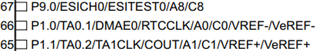
In my specific case, P9.0/ESICH0/ESITEST0/A8/C8, A8 appears to correspond to the secondary pin function. Therefore, I use section 12.2.5 of the User's Guide, and use the code below to set P9SEL1 to 1 and P9SEL0 to 0 for bit 0. The example code sets A1 with the tertiary function selection, so I assumed that I set A8 with the secondary function selection, but it is not working.
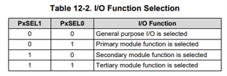
P9SEL1 |= BIT0;
P9SEL0 &= ~BIT0;
