


Other Parts Discussed in Thread: MSP-FET
Hi Team MSP,
A few questions on the bootloader for the F5242 WRT the F5242 Datasheet & SLAU319. We are having trouble starting the BSL/Bootloader on the F5242.
We put the F5242 into BSL mode w/ the datasheet specified pins "The BSL requires a specific entry sequence on the RSTDVCC/SBWTDIO and TEST/SBWTCK pins".. and the SLAU319 specified sequence (as shown below)..
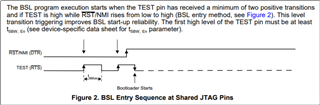
In our case.. "The width of the first pulse on TEST is about 66us. The second one is about 80us. The RSTDVCC signal rises at the middle of second TEST pulse signal."
Our entry sequence is shown below..
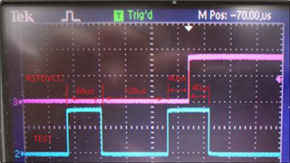
We are running a PC-USB/TTL dongle at the same voltage as the F5242 & @ 9600 Baud.
USB/TTL dongle TX(Output) connected to F5242-Pin1.2 & USB/TTL dongle RX(Input) connected to F5242-Pin1.1
SLAU319 says that if we send a simple "0x80" on the F5242 (P1.2) UART RX pin, we should get a "0x90" response on F5242 (P1.1) UART TX pin.. but we get no response from the F5242 on pin P1.1.
Thoughts?
SLAU319 Example Sequence says.. "TO BSL: 80.. FROM BSL: 90".
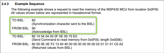
Is just an "80" sufficient to invoke a "90" response?
Or.. is a longer sequence actually required (say w/ a CMD etc) to evoke a response from the F5242?
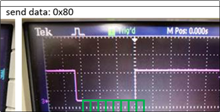
Here is our test input.. w/ the green markers showing the 8 data bits (0x80).. which go in as LSB first "0000_0001"
Additional questions..
To confirm..
Is the BSL "Start bit" a logic "0"? Is the BSL "Stop bit" a logic "1"?
Thanks, Merril