This thread has been locked.

If you have a related question, please click the "Ask a related question" button in the top right corner. The newly created question will be automatically linked to this question.

MSP430F5328: Failure on the ports of MCU

Part Number: MSP430F5328

Hi Team,

We have received this report from our customer,

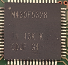
We have problems with a charge of your MSP430F5328 Microcontrollers. 

Some/Many Microcontrollers of this marking / charge seems to have a leakage current or something else, which leads to a fail behaviour. When the optokoppler is inactive the Voltage should be around 3.1V. In Fail PU.0 has 0V and PU.1 has 1.5V. Not all microcontrollers with the same marking are effected from this problem.

We've stopped the production, because of this issue. Please check and declare why there is a problem. 

Some devices starts running if a measurement is taken with a multimeter. Some starts running on contact with PU.0 some with PU.1.


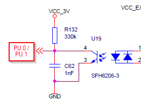
It seems the pull-up resistor is too high for this application. Can you please confirm?

Regards,

Danilo

  • Hello Danilo,

    Typical leakage current on a GPIO is ~50nA, but from the description, the customer is seeing 4.5uA (3v-1.5v)/330K or as much as 3v/330K = 9uA.

    To rule out the possibility of leakage current in the SFH6206-3, if the customer disconnected the pin#4 on this devices from the circuit, does the customer see same issue?

  • Hi Dennis,

    Thank you for your feedback. According to our customer, 

    This cannot be the problem, because we are using the same circuit on over 20 Pins without any problems.

    We think the problem is the LDO. Please send us extended information for the realationship of the PU-Ports and the LDOO / LDOI Pins.

    Regards,

    Danilo

  • Hi Danilo,

    I'm requesting additional information from our product/test team.

  • Hi Dennis,

    We will wait for your feedback.

    Thanks,

    Danilo

  • Hi Danilo,

    Apparently I need to reach out to our team in China for this, but it is a holiday this week.  I will see if there is someone in our India team that can help.

  • Hi Dennis,

    Thank you for the update. Looking forward to the product team's feedback.

    Regards,

    Danilo

  • Hi Danilo,

    I apologize this is taking longer than expected.  I have managed to contact the appropriate engineers in India.  They will be able to help look into this issue.

  • Hi Danilo,

    I apologize for the delay.  I have had to reach out to our team in India a second time for assistance.

  • Hi Danilo,

    While we wait for assistance from the product team, let's get some additional information.  Can you find out how the customer is enabling these pins?

    Can they provide the section of their code that performs the operations described below?

    Has the customer tried using a small resistor value?  say 100K or even 10K?  If so, what voltages to they see on the PU.0 and PU.1 pins?

  • Hi Dennis,

    Here is the response of our customer,

    Here is the inital code for Port U as Input:
    LDOKEYPID = 0x9628;
    PUCTL = PUIPE;
    LDOKEYPID = 0x0000; // lock register again

    Yes we've tried a smaller resistor and the problem seems to be gone. In fail we see different voltages with a multimeter. from 0V to 1,5V (See my start post), but the most cases starts running if the multimeter probe gets in contact with the pins.

    Regards,

    Danilo

  • Hi Danilo,

    I did get a response from one of our designers.

    Here are his comments:

    =======================

    This device is a USB device with disabled USB interface.

    For the USB devices we implemented a 5V to 3.3V LDO with 50mA load current. This LDO was intended to power the MSP430 when only USB power was available. In this case you connected the VBUS from the USB connector to the LDOI pin and the LDOO pin was connected to the AVCC/DVCC pins to power the MSP430.

    The PU.x pins are the 3.3V USB data pins and they are powered by the USB LDO output (LDOO). They have a 25mA load current capability. The USB protocol is defined as a differential voltage level on the D+/D- data pins. That is the reason the PU.0 / PU.1 pins can only be controlled together as input or output.

    Even if the PU.x pins are configured as an input, they must still be powered with a correct voltage on the LDOO pin. Other wise the input / output driver logic may not functioning correctly.  Check the LDOO supply first to make sure the I/O’s are powered correctly.

    If the supply is correct, and the configuration as an input is correct, there is not much that can go wrong. Specifically the input leakage cannot be an issue, unless they had an ESD event and damaged the silicon.

    ======================

    Danilo - How is the customer powering the LDO?  Perhaps they can share a larger portion of their schematic showing all of the MSP430 connections?

  • Hello Dennis,

    This is Dominik the customer who had contact with Danilo.

    In the actual layout LDOO and LDOI Pins are not connected, because we are just using the PU Pins as Inputs. Suppling the LDOO with 3,3V turns into a instable state with capacitive behaviours.

    In our tests a lower resistor as Pullup with 150kOhm seems to fix the problem, but we are not sure if we are working in a border area of thresholds?

    Please note that we already have used this schematics in hundreds of devices without any problems over more than 1 year.

    Best Regards

    Dominik

  • Hi AngelDP,

    Thank you for the information, and I apologize this is taking some time to nail down what is going on here.  Beyond the device datasheet and user guides, our team does not have access to the device's design documentation, which would tells us how things are wired up internally.  For this we have to reach out to one of our design engineers to help solve this mystery.  Unfortunately this is an older device and the original design engineer is no longer with TI.

    So to help our designer, let me make sure I have this correct - in your design you don't have anything (no voltage) applied to LDOO or LDOI, and if you do apply +3.3v to the LDOO pin and ensure that the LDO is disabled, the input pins appear to have some capacitive behaviours - correct?

  • Hello Dennis,

    Correct, but it is not ensured that the LDO is disabled. We don't touch the LDO Settings / Register. Is the LDO disabled per default? Maybe the "Ghost Effect" results out of an open LDOI and forced LDOO when the LDO is active?

    I could check if it would work, when the LDO is disabled, but this solution is very cost intensive for us, so we would prefer to solve the problem with the  lower resistor value. For that we would like to have a statement for that case!

    Dominik

  • Hello Dominik,

    I have passed your response along to the design engineer and I am waiting for his response.

    In the mean time, you indicate you don't touch the LDO settings.  By default the LDO is in fact enabled at power on.

    But, it appears, from the user guide, that if you tie LDOI low, then the LDO remains disabled. Do you tie LDOI low?

    Also note the comment about Port U requiring an external +3.3v on LDOO to use these pins properly.

    I suspect this may be the issue. As an experiment, can you confirm that if you apply a minimum of 3.76v on LDOI and after power-on you measure +3.3v on LDOO, then check for the leakage current on the Port U pins?

  • Hello Dominik,

    Our design engineer has come back with a response.

    =================================

    Not powering the LDOO explains the observed flaky behavior.

    Since the customer application is using a pull up on the PU.0 / PU.1 pins, the 3.1V level on the pin is powering the LDOO domain over I/O pad internal ESD diode. If you measure the LDO pin under these conditions the customer describes, you should see about 2.5V.

    That also explains, why a lower series resistor in the pull up path solves the problem. Now they are dumping more current into the ESD diode.

    The behavior can also be affected by temperature and will vary from device to device. If the customer has been using the device in this way they have been lucky, but there is no guarantee that a different lot of devices will behave the same.  This is why the particular device with the date code they show in the picture is not behaving in the same way.

    Unfortunately, at the end of the day without the LDOO pin properly connected, we  (TI) can not guarantee proper operation.

    =================================

  • Hello Dennis,

    So if we want to use the Port U as input/outut we either need to supply the LDOI with 3,76V - 5,5V or tie LDOI down to GND and supply LDOO with our existing 3,3V. Since we have no higher voltage than 3,3V we would choose the second method.

    Please confirm shortly if this is correct.

    Dominik

  • Hello Dominik,

    I wanted to check in with you to see if you had a chance to verify that the solution works for you.  I assume you will modify one of your existing units and test that applying the proper voltage fixes the problem.

  • Hi Dominik,

    It's been a few days since I have heard from you so I’m assuming your were able to resolve your issue.
    If this isn’t the case, please click the "This did NOT resolve my issue" button and reply to this thread with more information.
    If this thread locks, please click the "Ask a related question" button and in the new thread describe the current status of your issue and any additional details you may have to assist us in helping to solve your issues.

**Attention** This is a public forum