Hello,
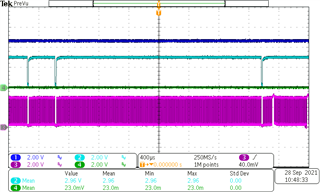
I am trying to control battery state control switches using GPIO pins. I used the same port but a different pin for setting PWM channels. However, my understanding is that these pins should not interfere with each other. However, even though my battery switch control output should be 1, it randomly goes to zero and turns back on. The pwm output also goes to low and high and sometimes this overlaps with the battery switch signal. Is there something wrong with the way I am configuring the pins? The code is supposed to sense the input voltage sensor value, trigger and ADC interrupt and enable or disable the battery switch. Thank you in advance.
code is below
initial code
/*
P1SEL |= BIT7; // Set P1.7 to output direction - High BUCK
P1DIR |= BIT7;
P2SEL |= BIT0; // Set P2.0 to output direction - Low BUCK
P2DIR |= BIT0;
P2SEL |= BIT2; // Set P2.2 to output direction - High BOOST
P2DIR |= BIT2;
P2SEL |= BIT3; // Set P2.3 to output direction - Low BOOST
P2DIR |= BIT3;
*/
// configure ADC pins
PMAPPWD = 0x02D52; // Enable Write-access to modify port mapping registers
PMAPCTL = PMAPRECFG; // Allow reconfiguration during runtime
P1MAP0|= PM_ANALOG; // Modify all PxMAPy registers - A0 - Iin
P1MAP1|= PM_ANALOG; // Modify all PxMAPy registers - A1 - Vout_buck
P1MAP2|= PM_ANALOG; // Modify all PxMAPy registers - A2 - Vout
P1MAP3|= PM_ANALOG; // Modify all PxMAPy registers - A3
P1MAP4|= PM_ANALOG; // Modify all PxMAPy registers - A4 - Vbat
P1MAP5|= PM_ANALOG; // Modify all PxMAPy registers - A5 - Iout
P3MAP5|= PM_ANALOG; // Modify all PxMAPy registers - A8 - Ibat
P3MAP6|= PM_ANALOG; // Modify all PxMAPy registers - A7 - Vin
P2MAP2|= PM_TD1_1;
P2MAP3|= PM_TD1_2;
P2MAP0|= PM_TD0_2;
P1MAP7|= PM_TD0_1;
P1SEL |=BIT7+BIT5+BIT4+BIT3+BIT2+BIT1+BIT0; // setting the port mapping register PxMAPy to PM_ANALOG together with PxSEL.y=1 when applying analog signals
P3SEL |=BIT6+BIT5;
P2SEL |= BIT0+BIT2+BIT3;
P2DIR |= BIT0+BIT2+BIT3;
P1DIR |= BIT7;
P3SEL &= (~BIT0); // Set P3.0 to GPIO and to output direction - BAT_GD_EN
P3DIR |= BIT0;
P2SEL &= (~BIT6); // Set P2.6 as GPIO and to output direction - Vgate BAT
P2DIR |= BIT6;
PMAPPWD = 0; // Disable Write-Access to modify port mapping registers by writing incorrect key
// main code
while (1)
{
SetADC(7);
GetADC(7);
}
// ADC10 interrupt service routine
#pragma vector=ADC10_VECTOR
__interrupt void ADC10_ISR(void)
{
switch(__even_in_range(ADC10IV,12))
{
case 0: break; // No interrupt
case 2: break; // conversion result overflow
case 4: break; // conversion time overflow
case 6: break; // ADC10HI
case 8: break; // ADC10LO
case 10: break; // ADC10IN
case 12:
ADC10CTL0 &= ~ADC10ON; // ADC10 disabled completely
ADC_Result= ADC10MEM0;
Vin_temp=ADC_Result;
if (Vin_temp>=Vin_min){
OffBattery();
SetDuty_Buck (D_buckH, D_buckL);
__delay_cycles(10); // Delay between sequence convs
}
else if(Vin_temp<Vin_min & Vin_temp>=Vin_minABS){
// turn off buck stage
OffBuck(0,0);
__delay_cycles(100); // Delay between sequence convs
OnBattery();
__delay_cycles(50); // Delay between sequence convs
// turn on the boost stage
SetDuty_Boost(D_boostH, D_boostL);
}
else if (Vin_temp<Vin_minABS)
{
OffBattery();
OffBuck(0,0);
OffBoost(0,0);
}
__bic_SR_register_on_exit(CPUOFF);
break; // Clear CPUOFF bit from 0(SR)
default: break;
}
}
void OnBattery(){
P3OUT |= BIT0; //set 3.0 to high - enable battery GD
P2OUT |= BIT6; //set 2.6 to high
}
void OffBattery(){
P3OUT &= ~BIT0; //set 3.0 to low - disable battery GD
P2OUT &= ~BIT6; //set 2.6 to low - disable battery FETs
}