This thread has been locked.

If you have a related question, please click the "Ask a related question" button in the top right corner. The newly created question will be automatically linked to this question.

MSP430FR2433: MSP430FR2433

Part Number: MSP430FR2433

Hi, 

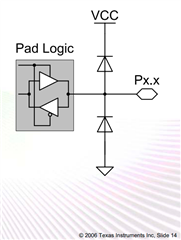
I have a GPIO pin which is configured input with a programed pull down.  

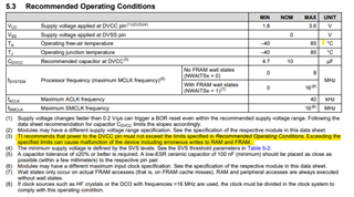
I'd like to ask what will happend if i give an input voltage more than Vcc+0.3 with Vccmax=3.2V.

There are internal protection in the GPIO? Because i feel that whatever the input voltage, i get only 4V at the GPIO pin.

Thank you

Best regards.

Liang  

  • Yes, there are internal ESD structures (diodes) on the pins to both VCC and GND. You are forward biasing a low power diode and will damage the device if you put a higher voltage than the Absolute Maximum stated in the datasheet.

  • Thank you for your relay. The absolute maximum value is a peak vleur of an anverage value? 

  • Any voltage above VCC+0.3 will start conduction on the diodes. You SHOULD NOT be applying ANY signals, peak or average, higher than VCC+0.3 if you want your MCU to have any kind of life span.

  • Hi Liang,

    Can I ask what your inputs are that you need to go over the recommended operating conditions? As Seth mentioned, any value crossing the absolute maximum ratings will damage your device.

    The recommended operating condition for VCC is maxed at 3.6 V and going above this can still cause damage. So if you have the absolute max input at the maximum recommended VCC you will still be under the 4V. 

    Would using a voltage divider to tune down your input signal be applicable in your application?

    Regards,

    Luke

  • Hi Luke, 

    The VCC is about 3.2V for our application. 

    My question concerne about the Voltage applied to GPIO. 

    The architecture aims to activate µC by set input high to a GPIO. 

    My input is an electromagnetic pulse, generated by the device's near-field antenna from an external signal generator. The stength of the input voltage depends on antenna's position which is random. 

    As shown in the figure, the R1 is µC internal configurated pull down.  The diode and the following capacitor is a half rectifier to transfert the input sinus signal to a smooth DC voltage. 

    I tried to divided the signal by set R4, but this cause activation no efficency.

    However, my µC doesn't looks like KO after serval activation test by GPIO. 

    What kind of errors can be caused if  Voltage applied to GPIO is higer than recommanded? 

    Thank you in advance 

    Best regards 

    Liang 

  • If you violate the absolute maximums, you bought the device.The point is TI can't tell you what might happen, because they don't do any testing there. If you burn out the ESD diode, you leave the chip unprotected.

**Attention** This is a public forum