This thread has been locked.

If you have a related question, please click the "Ask a related question" button in the top right corner. The newly created question will be automatically linked to this question.

MSP430FG6426: CTSD16 Conversion Time

Part Number: MSP430FG6426

I'm having trouble with the long CTSD16 conversion time.
Please tell me the reason.

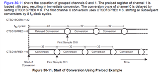
The main settings of CTSD are as follows.
Sampling rate = 32 clocks
PreloadValue=0 clock
CTSD16INTDLY=1b (First sample causes interrupt)
CTSD16RRI=1b (Rail-to-rail input enabled)
Continuous conversion mode
SMCLK=4MHz
The conversion result is stored in the buffer memory by DMA.
After conversion for the specified number of times, CTSD conversion is stopped by a DMA interrupt.

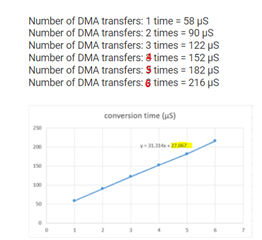
The time from the start of CTSD conversion to the stop of CTSD conversion by a DMA interrupt is shown below.

Number of DMA transfers: 1 time = 58 μS
Number of DMA transfers: 2 times = 90 μS
Number of DMA transfers: 3 times = 122 μS
Number of DMA transfers: 3 times = 152 μS
Number of DMA transfers: 3 times = 182 μS
Number of DMA transfers: 3 times = 216 μS

The vertical axis is the conversion time, and the horizontal axis is the number of DMA transfers.

Approximately 27µS is added to all conversion times.
What do you think is the reason for adding this 27μS?

  • I think the 27us is added only on the first conversion. Can you show how you show DMA trigger frequencies? Using GPIO?

  • Thank you for your reply.
    DMA trigger is set to CTSD16IFG0.
    After setting the trigger, CTSD conversion is started.
    I am using DMA2.
    Did you get the answer above?

    For reference, the code when setting the DMA trigger is as follows.

       DMA2SZ = repnum;
       DMA2SA = Address of CTSD16MEM0 
       DMA2DA = Address of Strage Memory
       DMACTL1 |= (DMA2TSEL4 + DMA2TSEL3);
       DMA2CTL |= DMAEN;
       usReadReg = CTSD16MEM0;      // overflow prevention
       CTSD16CCTL0 |= CTSD16SC;    // CTSD16 start conversion

    Thank you.

  • Hi,

    1. Will the time will influence your application?

    2. I think you make a little mistake:

    3. My question is that how you know the DMA start working and finish working? How you measure the time?

    Eason

  • thank you for your reply.

    >1. Will the time will influence your application?
    I'm sorry. I'm not good at English and I can't understand your question well enough.
    The question is "Does the timing of the CTSD16 conversion start change depending on the timing of the application?" …the answer is NO.
    The measured data in the graph was Waited with nop from CTSD16 conversion to DMA transfer completion.

    >2. I think you make a little mistake:
    I'm sorry. It is as you pointed out.

    >3. My question is that how you know the DMA start working and finish working? How you measure the time?
    I output a signal to GPIO and measured it with an oscilloscope.
    HIGH is output to GPIO at the start of CTSD conversion, and LOW is output at the DMA transfer completion interrupt.
    I measured the GPIO HIGH period with an oscilloscope.

  • See from the result, I think only the first conversion time is added 27us, for the next conversions, the time is right about 32us.

    I would assume there may be some problem with the Sigma delta ADC. As I know, SD ADC will have some delay time because of the sinc3 filter, it is not a runtime ADC, like SAR ADC.

  • My question is will this delay affect your project?

  • Thank you for your advice to delay ADC conversion start to first ADC completion by 27μS due to sigma delta ADC.
    This delay will affect the project.
    I'm thinking of taking measures to advance the start of ADC conversion uniformly by 27 μs.

  • What about ignore the first conversion result?

    You may be need this function as well:

**Attention** This is a public forum