This thread has been locked.

If you have a related question, please click the "Ask a related question" button in the top right corner. The newly created question will be automatically linked to this question.

MSP430F6779: MSP430F6779 Measuring Voltage of PWM signal

Part Number: MSP430F6779
Other Parts Discussed in Thread: TIDM-THREEPHASEMETER-F6779

I am developing code for a level 2 electric vehicle car charger. I am using the example code from the Three Phase power meter(TIDM-THREEPHASEMETER-F6779).

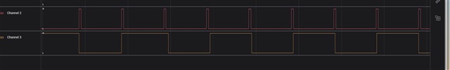
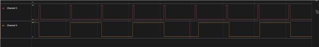
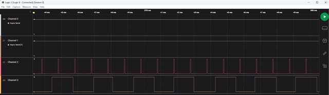
I am generating a PWM signal using Timer 2 as shown in the code below. I am trying to measure the voltage of the PWM signal at a 5% duty cycle. The picture below shows the PWM signal on top and then the bottom is a pin I am toggling to show when the ADC will sample the PWM signal. 

Why doesn't the TIMER2_A0 interrupt fire every time the Timer reaches TA2CCR0? Shouldn't TIMER2_A0 interrupt fire right when the PWM signal goes from low to high?

Is there a better way to measure the voltage of the PWM signal? 

/* Set Initial PWM Period 1kHz */
TA2CCR0 = 16685 - 1; //32786 Hz clock divided by 2 with some offset. The -1 comes from timer counting from 0 and not 1.

/* CCR0 reset/set */
TA2CCTL1 = OUTMOD_7;

TA2CCTL0 = CCIE; // CCR0 interrupt enabled

CURRENT_RATING = 5.0;
CURRENT_RATING = CURRENT_RATING / 100.0;
TA2CCR1 = 16685.0 * CURRENT_RATING;

/* SMCLK, up mode, clear TAR */
TA2CTL = TASSEL_2 | MC_1 | TACLR | TAIE;

/******* Enable Pilot Wire PWM ******/
P11DIR |= BIT3;
P11SEL0 |= BIT3;
P11OUT &= ~BIT3;

#pragma vector=TIMER2_A0_VECTOR
__interrupt void Timer2_ISR (void)
{
P9OUT ^= BIT0; //Toggle pin
ADC10CTL0 |= ADC10ENC + ADC10SC;
}

Thanks for the help,

Mike

  • What is your TIMER2_A1_VECTOR doing? I wonder if it's blocking/delaying the CCR0 interrupt.

    I'm not quite sure what "measuring the voltage of the PWM" means, since a PWM signal is digital. Are you interested in measuring duty cycle?

  • Thanks for the reponse Bruce. Below is Timer2_A1_vector. However, I just moved the code from TIMER2_A0_VECTOR to the TA2IV_TA2IFG case to get the picture below. It seems to be a little better, but you can see that in some cases P9.0 transitions outside of when the PWM signal is high. I am trying to read the analog input of the PWM signal when the PWM signal is high to measure the voltage.   

    For electric car charging, the electric car will pull the PWM signal down from 3.3V to 2.7V when plugged into the car charger. When the car is ready to charge,  the PWM signal will get pulled down to 2.1V. This PWM signal is going to an analog input pin. Does that make sense? I am generating the duty cycle so I already know what the duty cycle is. The duty cycle determines how much current the electric car can pull from the charger.   

    // Timer2_A1 Interrupt Vector (TAIV) handler
    #if defined(__TI_COMPILER_VERSION__) || defined(__IAR_SYSTEMS_ICC__)
    #pragma vector=TIMER2_A1_VECTOR
    __interrupt void TIMER2_A1_ISR(void)
    #elif defined(__GNUC__)
    void __attribute__ ((interrupt(TIMER2_A1_VECTOR))) TIMER2_A1_ISR (void)
    #else
    #error Compiler not supported!
    #endif
    {
    switch (__even_in_range(TA2IV, 14))
    {
       case TA2IV_NONE: break; // No interrupt
       case TA2IV_TA2CCR1: break; // TA0CCR1_CCIFG
       case 4: break; // Reserved
       case 6: break; // Reserved
       case 8: break; // Reserved
       case 10: break; // Reserved
       case 12: break; // Reserved
       case TA2IV_TA2IFG:
          P9OUT ^= BIT0; //Toggle pin
          ADC10CTL0 |= ADC10ENC + ADC10SC;
          break; // TA0IFG
       default: break;
    }
    }

  • Oh, OK, it sounds like you really do want to measure the (high-side) voltage of the PWM. (I hadn't seen that before.)

    This new trace seems to show (more or less) normal latency for the TAIFG interrupt, due both to other system activity and to the time it takes to enter the ISR. (The difference is there's jitter but no obvious drift.) This latency is one of the hazards of using a software-based start for the ADC.

    Skipping to the end: If you can, I suggest using TA3 rather than TA2. TA3.0 (i.e. CCR0) can provide a hardware trigger for the ADC via ADC10SHS=2 [Ref data sheet (SLAS768E) Table 6-20], so you avoid all the software/ISR latency.

    Background: It looks like your sample/PWM period is about 1msec, so a 5% duty is about 50usec. Even if you reduce the latency, you still have to make sure your ADC start+sample/hold can complete in that time. This takes into account ISR latency(max) and ADC10SHT / ADC10SSEL. This is somewhat tight, and variable latency makes it more difficult. If you can reduce the latency to 0(max) using ADC10SHS, you just have to adjust ADC10SHT/ADC10SSEL (statically) to complete in 50usec.

  • Yes, I am trying to measure the high side voltage of the PWM signal and this high side voltage will change throughout a car charging session. The PWM signal is a 1kHz signal. 

    Can I input this PWM signal into a port 1 pin and use the rising edge to trigger the ADC? Or will there be too much delay in trying to do this?

  • When you say TA3.0 (i.e. CCR0) can provide a hardware trigger for the ADC, then the ADC will automatically trigger when TA3 reaches CCR0?

    So I won't have to do this ADC10CTL0 |= ADC10ENC + ADC10SC;  in software ??

  • Yes. You would need to move your PWM from P11.3 (TA2.1) to P11.1 (TA3.1) and set ADC10SHS=2. And change your TA2 config code to TA3. (You won't need the ISR.)

    In your ADC10 ISR, you'll need to toggle ADC10ENC (=0, then =1) [Ref UG (SLAU208Q) Sec 27.2.7.1] after each conversion.

  • I am not able to get the ADC10 ISR to trigger at all using ADC10SHS=2. Below is the Timer3 code and ADC10 setup code. I put a breakpoint in the ADC ISR but it never triggers. 

    TA3CCR0 = 16685 - 1; //32786 Hz clock divided by 2 with some offset. The -1 comes from timer counting from 0 and not 1.

    /* CCR0 reset/set */
    TA3CCTL1 = OUTMOD_7;

    //TA3CCTL0 = CCIE; // CCR0 interrupt enabled

    CURRENT_RATING = 5.0;
    CURRENT_RATING = CURRENT_RATING / 100.0;
    TA3CCR1 = 16685.0 * CURRENT_RATING;

    /* SMCLK, up mode, clear TAR */
    TA3CTL = TASSEL_2 | MC_1 | TACLR;// | TAIE;

    ADC10CTL0 &= ~ADC10ENC;
    /* Clear pending interrupts to ensure trigger for DMA */
    ADC10IFG = 0;

    /* ADC on, ADC10 waits for trigger from the SD24, sampling time 2us 8xADCclk, auto next conv. */
    ADC10CTL0 = ADC10SHT0 | ADC10ON | ADC10MSC;

    /* Triggered by the SD24, SMCLK/6 = 4MHz, Pulse Sample Mode*/
    ADC10CTL1 = ADC10SHP | ADC10SHS_2 | ADC10DIV_0 | ADC10SSEL_0 | ADC10CONSEQ_0; /* Single Channel, Single Conversion */

    /* 10-bit conversion results */
    ADC10CTL2 |= ADC10RES;

    /* Enable ADC conv complete interrupt */
    ADC10IE |= ADC10IE0;

    /* A3 ADC input select; Vref=AVCC */
    ADC10MCTL0 |= ADC10INCH_3 | ADC10SREF_0;

    /* Enable ADC10 interrupts */
    //ADC10IE = ADC10IE0 | ADC10OVIE | ADC10TOVIE;

    /* Start ADC and wait for a software start conversion trigger */
    ADC10CTL0 |= ADC10ENC;// + ADC10SC;

  • Sorry, I forgot for a moment that the TA3.0 trigger relies on the TA3.0 signal, not the IFG. The CCR0 signal can really only be Toggle, at half the frequency, but the trick is to reverse the trigger sense each time, so each CCR0 event triggers. 

    So add to the configuration sequence:

    > TA3CCTL0 = OUTMOD_4;   // Toggle at half-frequency; ISSH reversal (see ISR) gives full frequency

    Then when you toggle ENC in the ISR:

    >  ADC10CTL0 &= ~ADC10ENC;    // Toggle ENC per UG Sec 27.2.7.1
    >  ADC10CTL1 ^= ADC10ISSH;       // Toggle ISSH to provide trigger on each cycle (EQU0)
    >  ADC10CTL0 |= ADC10ENC;

    I don't have an F6779, but I just did this combination on an F5529 (ADC12) using TB0.0.

  • After adding that code, the ADC10 ISR still never gets triggered. Right now, I don't have any ISR code for TA3, not sure if that matters or not. Below is the ADC10 ISR code now for your reference. Let me know if you want me to check any TA3 registers or add breakpoints or anything to help troubleshoot this. 

    ISR(ADC10, adc10_interrupt)
    {
       switch (__even_in_range(ADC10IV, ADC10IV_ADC10IFG))
       {
          case ADC10IV_NONE:
             break;
          case ADC10IV_ADC10OVIFG:
             break;
          case ADC10IV_ADC10TOVIFG:
             break;
          case ADC10IV_ADC10HIIFG:
             break;
          case ADC10IV_ADC10LOIFG:
             break;
          case ADC10IV_ADC10INIFG:
             break;
          case ADC10IV_ADC10IFG:
             ADC10CTL0 &= ~ADC10ENC;
             ADC_Result = ADC10MEM0; // Store ADC10 channel 0 result
             ADC10CTL1 ^= ADC10ISSH; // Toggle ISSH to provide trigger on each cycle (EQU0)
             ADC10CTL0 |= ADC10ENC;
             break;
          }
    }

  • The Usual Suspects:

    1) Are you enabling GIE somewhere? (__enable_interrupt())

    2) Can you monitor TA3.0 (P4.7 configured per data sheet table 6-76)? It should look like a square wave at 1/2kHz.

    3) If you pause the program, where is it executing (unexpected wrong turn somewhere)?

    4) At program startup, use the debugger to set ADC10MEM0 to something distinctive (e.g. 0x123) then run, then see if it changes. This will divide the trigger-the-ADC step from the completion-interrupt step.

  • This code is from the three phase power meter example code here, which I have modified for my application.  www.ti.com/.../TIDM-THREEPHASEMETER-F6779

    1. I searched and couldn't find this, but IAR doesn't search all files for some reason. I also added this to the code, but the ADC ISR still isn't getting triggered by TA3. 

    2. I soldered a wire to TA3.1 yesterday and see the PWM signal on it. It took a long time to do this since my soldering iron is big and I kept shorting pins next to it. I can do this if you would like me to though. 

    3. When I pause the program it looks normal. When I run and pause a few times, it isn't getting stuck on one line of code. 

    4. I did this, but when I pause the program this value never changes. I also have breakpoints in my ADC ISR and they never get triggered.   

  • 1) It sounds like you're modifying a larger code base. I wonder if some other code is using TA3. Try searching for e.g. TA3CTL.

    2) Glancing at the schematics in SLAA577G, I think you'll be able to see P4.7 on the low side of R59, next to LED4. (It will also blink the LED, but too fast to see.)

  • I didn't realize pin access was quite so difficult on your platform. Another option is to use TA0.1 (AD10SHS=1) for your PWM. That signal comes out on pin P2.1, which is connected to one of the RF Daughter Card headers (RF_CS, pin RF2.14). Those tiny pins are a bit of a pain to work with, but probably less so than the MCU pins. [Edit: Is anything in your program using TA0?]

  • We actually made our own custom power meter board from this reference design so a lot of the pins don't go anywhere on the board and we don't use the RF daughter cards or LCD or LED4 that you mention. We are modifying our power meter board that has been in production for a few years to be the main system controller board with an integrated power meter. Hope that helps clear things up. 

    I ordered a microscope that just came in since I wasted a lot of time the other day. I will solder a wire to TA3.0 and let you know what it looks like. 

    There isn't any other code using TA3. I checked that before changing the TA2 code to TA3. 

    Yes, TA0 is being used to drive the Sigma Delta ADC module to measure the voltage and current for the power calculations. 

  • I see a "_EINT()"  down near the end of system_setup().

    The fact that ADC10MEM0 didn't change indicates that indeed the triggering isn't happening. If it's useful, I can post the program I ran on the F5529 (it's only 72 lines). I don't have an F5-series device with an ADC10, but the F5-series ADC10 and ADC12 have many similarities.

  • I soldered a wire to TA3.0 P4.7 and I don't see anything on that pin. 

    It looks like the TA3 is counting because I see TA3R change. 

  • 1) Does TA3CCTL0 have OUTMOD=4 set?

    > TA3CCTL0 = OUTMOD_4;

    2) Did you configure P4.7 according to Table 6-76? Looking again, it claims P4DIR.7 is don't-care but I don't believe it.

    > P4SEL0 |= BIT7;  // P4.7 as PM_TA3.0

    > P4DIR |= BIT7;     // Output (notwithstanding the don't-care in Table 6-76)

    Step (2) is only for diagnosis -- it doesn't affect the triggering.

    [Edit: Fixed CCTL goof]

  • Yeah, I configured P4.7. I didn't see anything at first so I switched it to a digital pin and was able to toggle it high and see it work, just to verify I soldered the wire to the correct pin. Below is my current code. Cool you can edit responses. I see you changed TA3CCTL0 = outmod4. 

    Note that I don't have interrupts enabled on TA3 not sure if that matters. 

    TA3CCR0 = 16685 - 1; //32786 Hz clock divided by 2 with some offset. The -1 comes from timer counting from 0 and not 1.
    /* CCR0 reset/set */
    TA3CCTL1 = OUTMOD_4; // Toggle at half-frequency; ISSH reversal (see ISR) gives full frequency
    //TA3CCTL0 = CCIE; // CCR0 interrupt enabled
    CURRENT_RATING = 5.0;
    CURRENT_RATING = CURRENT_RATING / 100.0;
    TA3CCR1 = 16685.0 * CURRENT_RATING;
    /* SMCLK, up mode, clear TAR */
    TA3CTL = TASSEL_2 | MC_1 | TACLR;// | TAIE;

    /******* Setup P4.7 TA3.0 pin ******/
    P4SEL0 |= BIT7; // PxSEL - Peripheral function = 1, I/O = 0
    P4DIR |= BIT7; // PxDIR - Output = 1, Input = 0

  • TA3CCTL1 = OUTMOD_4; // Toggle at half-frequency; ISSH reversal (see ISR) gives full frequency

    This should be:

    > TA3CCTL0 = OUTMOD_4; // Toggle at half-frequency for ADC; ISSH reversal (see ISR) gives full frequency

    > TA3CCTL1 = OUTMOD_7; // PWM Reset/Set

  • Now the ADC10 ISR triggers!! :) Woohoo!

    Below is a picture of the timing. The top is the duty cycle and the bottom is a pin toggled in the ADC10 ISR. It looks like every 11 to 15 samples, the timing gets off and the ADC ISR doesn't trigger right at the high side of the PWM signal which is weird now that we are using a hardware trigger instead of a software trigger. Is there a way to fix this?

  • The ADC ISR is susceptible to the same latency as your earlier timer ISR, so wiggling a GPIO in the ISR isn't really definitive.

    The ADC is deterministic (give or take one ADC clock (200ns) for synchronization): Once triggered it spends ADC10SHT ticks (8 in your case) of the ADC clock (5MHz in your case) in sample/hold, then 12 ADC clocks converting, so about (8+12)/5=4usec. You only really care about the sample/hold, so your critical moment is 12 ADC clocks before the interrupt triggers, but that's an unknown time prior to the ISR actually executing.

    Due to the deterministic behavior, I think you're most interested in the case where channel 3 triggers earliest -- that gives you an upper bound on how long the conversion takes.

    It's possible to see more detail by monitoring ADC10CLK on a pin (P1.3, which is unfortunately also A3). I did this once on an F2 series device, and I could really see the clock start and stop for running the ADC. (I vaguely recall it kept running for 2-3 ticks after the ADC was done.) I don't know whether this experiment is worth the trouble, though.

    Do you see proper sample data? I'm still wondering about your source impedance, since SHT=1 is pretty short.

  • I am not too sure what is going on now with the code below. Now, I am not able to change the duty cycle of the PWM signal at all like before. I had to change the TA3CCR0 and TA3CCR1 value in order to get the PWM signal back to 1kHz, which is required for electric car charging. When I try and change the TA3CCR1 to a different duty cycle, it doesn't change it is always stuck at 50% duty cycle. I need to be able to change the duty cycle between 5% to 96% duty cycle. 

    TA3CCR0 = 8350 - 1;
    //TA3CCR0 = 16685 - 1; //32786 Hz clock divided by 2 with some offset. The -1 comes from timer counting from 0 and not 1.
    /* CCR0 reset/set */
    TA3CCTL0 = OUTMOD_4; // Toggle at half-frequency; ISSH reversal (see ISR) gives full frequency
    TA3CCTL1 = OUTMOD_7; // Toggle at half-frequency; ISSH reversal (see ISR) gives full frequency
    CURRENT_RATING = 95.0;
    CURRENT_RATING = CURRENT_RATING / 100.0;
    TA3CCR1 = 8350.0 * CURRENT_RATING;
    TA3CTL = TASSEL_2 | MC_1 | TACLR; /* SMCLK, up mode, clear TAR */

  • The "50% duty" observation sounds like you're probing TA3.0 (P4.7), not TA3.1 (P11.1). The scope trace above (top line) looks right for TA3.1.

    The PWM is on TA3.1 (P11.1). The TA3.0 (P4.7) probe was only for diagnosis.

  • Yeah, your right. I was freaking out for a second. lol I wasn't seeing anything on P11.1 so I probed P4.7 late last night. I just set P11.1 to a digital I/O and set it high and don't see anything so I need to resolder the wire to the chip again.  

  • [Side note: I don't know my schedule over the next week or so. There are plenty of smart people here to help, though you might find you have to start a new thread to get their attention.]

  • No worries Bruce. I resoldered the wire to P11.1 and it looks like everything is working fine now! Was worried for a minute. The measurements also look really stable now too. I need to do some more testing, but I have tested a 5% duty cycle, 50% and 96% duty cycle and it is looking pretty good! :)

    One other question. I also need to measure the low side of the PWM signal, is there something from TA3 that can trigger the ADC on the falling edge of the PWM signal at all? 

  • You're already using both of the TA3.0 edges (that's what the ISSH trick does), so I don't see another trigger mechanism. Using TA0.1 as the trigger you could use both edges of the PWM (using the ISSH trick, albeit with a race), but it sounds like that's not one of the choices.

    There may be a DMA trick possible (using the DMA to copy something into ADC10CTL0), though I'm not sure I could design it off the top of my head.

  • Okay, that makes sense. 

    I also need to read in more analog channels. Is there a good example for that somewhere? 

  • Example MSP430F677x_ADC10_10.c samples from A2 down to A0. With CONSEQ=1, the sampling goes from INCH down to A0. The example uses the DMA since otherwise the samples (typically) arrive too fast for the ADC ISR to pick them up in time.

    https://dev.ti.com/tirex/explore/node?node=A__AJYbjTaJ3i6izwfAKTplkg__msp430ware__IOGqZri__LATEST

  • Awesome, thanks for the help. When sampling multiple channels, would the ADC ISR go away and I would just have the DMA ISR and put the code below in the DMA ISR?

    ADC10CTL0 &= ~ADC10ENC;
    ADC10CTL1 ^= ADC10ISSH; // Toggle ISSH to provide trigger on each cycle (EQU0)
    ADC10CTL0 |= ADC10ENC;

  • Yes, in that case the DMA ISR indicates the completion, so you would do the ADC stuff there.

**Attention** This is a public forum