Other Parts Discussed in Thread: MSP432E401Y
Tool/software:
Hi teams:
I use TM4C1290 and MSP430 chips for SPI communication. TM4C is the host and MSP430 is the slave. The original configuration is mode 0, clock polarity is 0, phase is 0. Now the communication mode of the two chips is changed to clock polarity is 0, phase is 1, but the two chips cannot communicate normally.
MSP430 related definitions:
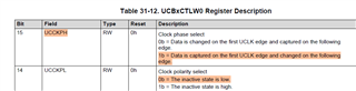
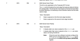
#define UCCKPH (0x8000) /* Clock phase select */
#define UCCKPH_H (0x0080)
#define UCCKPH_0 (0x0000) /* Data is changed on the first UCLK edge and captured on the
following edge. */
#define UCCKPH_1 (0x8000) /* Data is captured on the first UCLK edge and changed on the
following edge. */
TM4C related definitions:
#define SSI_FRF_MOTO_MODE_0 0x00000000 // Moto fmt, polarity 0, phase 0
#define SSI_FRF_MOTO_MODE_1 0x00000002 // Moto fmt, polarity 0, phase 1
#define SSI_FRF_MOTO_MODE_2 0x00000001 // Moto fmt, polarity 1, phase 0
#define SSI_FRF_MOTO_MODE_3 0x00000003 // Moto fmt, polarity 1, phase 1
//Before:
//Master:
SysCtlPeripheralEnable(SYSCTL_PERIPH_SSI1);
SysCtlPeripheralEnable(SYSCTL_PERIPH_GPIOE);
SysCtlPeripheralEnable(SYSCTL_PERIPH_GPIOB);
GPIOPinConfigure(GPIO_PB5_SSI1CLK);
GPIOPinConfigure(GPIO_PB4_SSI1FSS);
GPIOPinConfigure(GPIO_PE4_SSI1XDAT0);
GPIOPinConfigure(GPIO_PE5_SSI1XDAT1);
GPIOPinTypeSSI(GPIO_PORTE_BASE, GPIO_PIN_4 | GPIO_PIN_5 );
GPIOPinTypeSSI(GPIO_PORTB_BASE, GPIO_PIN_4 | GPIO_PIN_5 );
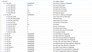
SSIConfigSetExpClk(SSI1_BASE, g_ui32SysClock, SSI_FRF_MOTO_MODE_0,
SSI_MODE_MASTER, 1000000, 8);
SSIEnable(SSI1_BASE);
//Slave:
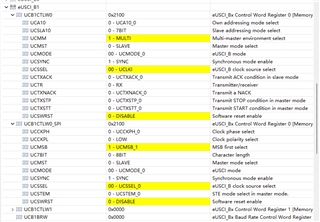
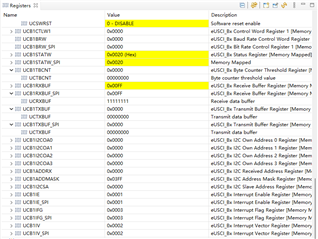
UCB1CTLW0 = UCSWRST; // **Put state machine in reset**
UCB1CTLW0 |= UCCKPH | UCCKPL_0 | UCMSB | UCSYNC| UCMST_0;
UCB1CTLW0 &= ~UCSWRST;
UCB1IFG &= ~(UCTXIFG | UCRXIFG);
UCB1IE |= UCRXIE;
//Now:
//Master:
SysCtlPeripheralEnable(SYSCTL_PERIPH_SSI1);
SysCtlPeripheralEnable(SYSCTL_PERIPH_GPIOE);
SysCtlPeripheralEnable(SYSCTL_PERIPH_GPIOB);
GPIOPinConfigure(GPIO_PB5_SSI1CLK);
GPIOPinConfigure(GPIO_PB4_SSI1FSS);
GPIOPinConfigure(GPIO_PE4_SSI1XDAT0);
GPIOPinConfigure(GPIO_PE5_SSI1XDAT1);
GPIOPinTypeSSI(GPIO_PORTE_BASE, GPIO_PIN_4 | GPIO_PIN_5 );
GPIOPinTypeSSI(GPIO_PORTB_BASE, GPIO_PIN_4 | GPIO_PIN_5 );
SSIConfigSetExpClk(SSI1_BASE,g_ui32SysClock,SSI_FRF_MOTO_MODE_1,SSI_MODE_MASTER, 1000000, 8);
SSIEnable(SSI1_BASE);
//Slave:
UCB1CTLW0 = UCSWRST; // **Put state machine in reset**
UCB1CTLW0 |= UCCKPH_0 | UCCKPL_0 | UCMSB | UCSYNC| UCMST_0;
UCB1CTLW0 &= ~UCSWRST;
UCB1IFG &= ~(UCTXIFG | UCRXIFG);
UCB1IE |= UCRXIE;