This thread has been locked.

If you have a related question, please click the "Ask a related question" button in the top right corner. The newly created question will be automatically linked to this question.

MSP430F2350 crystal oscillator Xout and Xin signals

Other Parts Discussed in Thread: TSS721A, MSP430F2350, MSP430F4793

Hi;

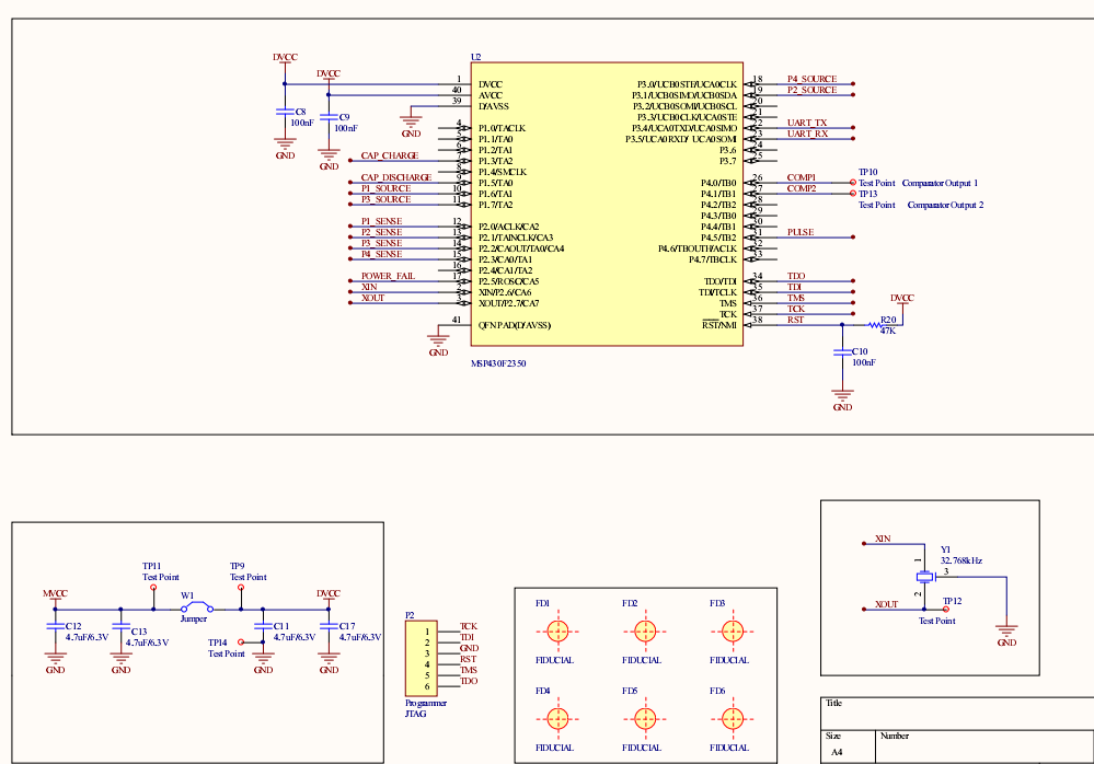
We are using  MSP430F2350 with a 32768Hz tuning fork crystal from Citizen:CFS-206 on our metering modules. No external load capacitors are connected,but internally XCAPX =3.We mounted the modules and after a while( 1months later),we could not communicate with some of  them via M-bus.We are using TSS721A  M-bus IC  on slave (our modules)

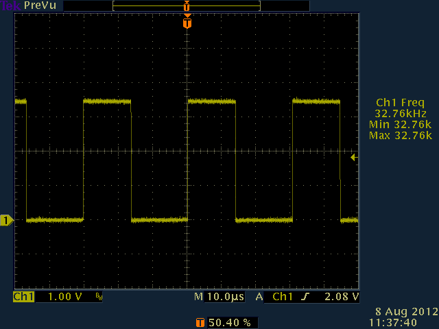
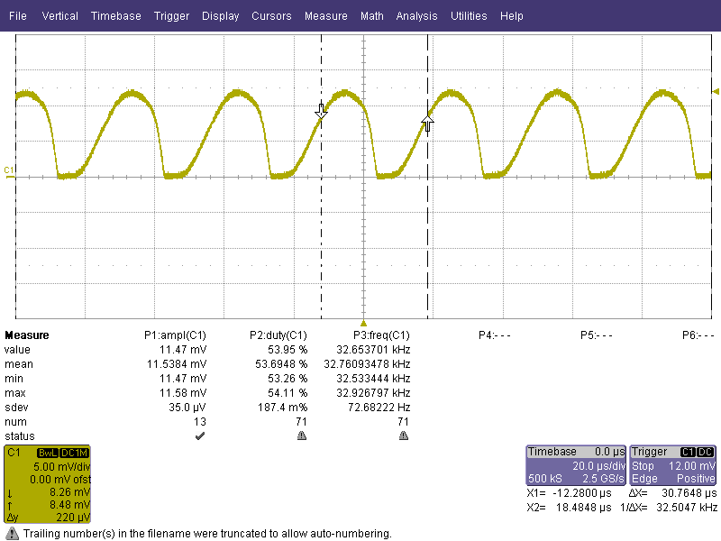
We suspected from XOSC8 erratum.Thus we made some measurements over crystal.ACLK duty cycle is measured to be  > %30 and  < %50

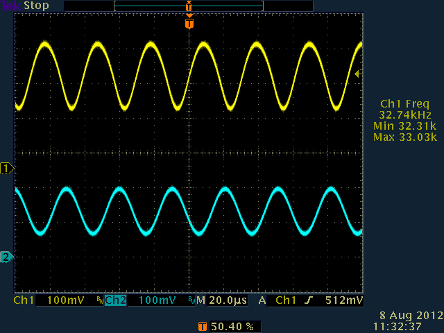
There exists a distorted and saturated sine wave signal at Xout pin.Xin signals looks as a sine wave. Please find the images below(please note that scale is 5mV and measurement is done via  X100 probe ,each square equals 500mV)

Xin:

Xout:

I have a few questions about crystal:

Are these  signals seem okay for a stable oscillation?Does  the pierce oscillator inside the mcu damp the signal such that after a while  ACLK falls below %30 duty?

Is there an overdrive issue exist due to saturating the crystal?

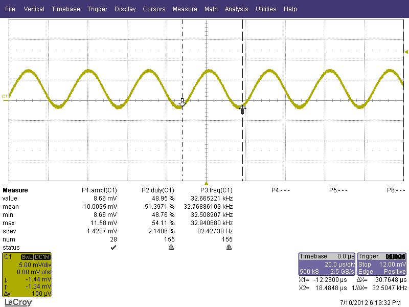
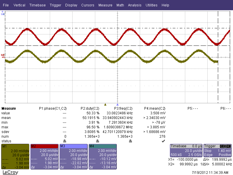
We use same crystal with another TI mcu:MSP430F4793 and the Xin(yellow) and Xout(red) signals given below(please note that scale is 2mV and measurement is done via  X100 probe ,each square equals 200mV)

Thank you

  • The Xout wave form of the F2350 doesn't really look nice. It might also be related to the design layout. You can check the MSP430 32-kHz Crystal Oscillators (Rev. B)
    for more detailts on the layout considerations.

    How do you configure the LFXT1 in your code?

    Is the OFIFG Flag set?

    Can you provide the schematic of your design?

    Which device revision do you use? The XOSC8 bug is already fixed on Rev. G devices.

    BR,

    Mo.

  • Dear Mo;

    Please find the code below:

    void halMcuInit(void)        //1 MHz from int dco
    {
        uint16 i;

        __bis_SR_register (OSCOFF);
        if ((CALBC1_1MHZ == 0xFF) || (CALDCO_1MHZ == 0xFF))   //calibration data are stored at the end of the information memory like 10ff                                  
        {  
            while(1);                               // If calibration constants erased
            // do not load, trap CPU!!
        }  


    /**
    *   BCSCTL3 BIT2 BIT3 usage 32768-Hz crystal on LFXT1
    *   Oscillator capacitor selection. These bits select the effective capacitance seen by the LFXT1 crystal when
    *    XTS = 0. If XTS = 1 or if LFXT1Sx = 11 XCAPx should be 00
    */
    #if defined (USE_INTERNAL_CAP)
    #if defined (USE_VLO_AS_REFERENCE)
        BCSCTL3 = LFXT1S_2;//  + XCAP_3;
    #else
        BCSCTL3 = LFXT1S0 + XCAP_3;            //LFXT1 32khz, 12.5pF cap selected
    #endif
    #else
        BCSCTL3 = LFXT1S0 + XCAP_0;          //LFXT1 32khz, 0 pF cap selected
    #endif        
        
        BCSCTL2 = 0x00;                    //MCLK ve SMCLK ource by DCO dividers 0, DCO resistor is internal
        BCSCTL1 = CALBC1_1MHZ | XT2OFF & (~XTS);       //XT2 off, XT1 low freq mode , ACLK DIV = 1, DCO range selected 1 mhz calibration value               
        DCOCTL = CALDCO_1MHZ;                //DCOx MODx calibrated values
        __bic_SR_register(OSCOFF);    


        // Wait for DCO to synchronize with ACLK (at least 28*32 ACLK cycles)
        for (i = 0x2000; i > 0; i--) asm(" NOP");
        // Wait for osc fault
        
        while (IFG1 & OFIFG)
        {
            // Clear oscillator fault flag
            IFG1 &= ~OFIFG;
            for (i = 0x64; i > 0; i--) asm(" NOP");
        }
        IFG1 = 0;

        
    }

    And schematic is:

    Thank you

  • unfortunately I am not able to see the schematic.

    However, can you please try to run the below simple code to see wheter anything changes?

    You should be able to see ACLK at P2.0 and MCLK at P1.2 (1MHz).

    #include "msp430f2350.h"
    volatile unsigned int i;
    void main(void)
    {
    WDTCTL = WDTPW + WDTHOLD; // Stop WDT
    P2DIR |= BIT0; // P2.0 = output direction
    P2SEL |= BIT0; // P2.0 = ACLK function
    P1DIR |= BIT2; // P1.2 = output direction
    P1SEL |= BIT2; // P1.2 = MCLK function
     
    //Setup 32kHz Crystal
    BCSCTL3 |= LFXT1S0 + XCAP_3; //LFXT1 32khz, 12.5pF cap selected
    do
    {
    IFG1 &= ~OFIFG; // Clear OSCFault flag
    for (i = 0xFF; i > 0; i--); // Time for flag to set
    }
    while (IFG1 & OFIFG); // OSCFault flag still set?
    //Setup DCO at 1MHz
    DCOCTL = 0x0; //Select lowest DCOx
    //and MODx settings
    BCSCTL1 = CALBC1_1MHZ; //Set range
    DCOCTL = CALDCO_1MHZ; //Set DCO step + modulation
    for (;;); // Infinite loop
    }

    BR,
    Mo.
  • Dear Mo;

    I attached the schematic.I also checked the version and it is written G4 on the  bottom right corner of the chip

    I will try the code as soon as possible

    Thank you

  • Dear Mo;

    We tried the code but nothing had changed.We were able to observe ACLK but we could not observe MCLK-1MHz signal at pin 6.

    I used TI's 40 pin target board for MSP430F23x0 family.

    May I ask you to send the hex code?

    Thanks

  • Sorry my mistake.

    SMCLK is on P1.4 (pin 8). SMCLK = MCLK in this scenario.

    Please try the below code:

    #include "msp430f2350.h"
    volatile unsigned int i;
    void main(void)
    {
    WDTCTL = WDTPW + WDTHOLD; // Stop WDT
    P2DIR |= BIT0; // P2.0 = output direction
    P2SEL |= BIT0; // P2.0 = ACLK function
    P1DIR |= BIT4; // P1.4 = output direction
    P1SEL |= BIT4; // P1.4 = SMCLK function
     
    //Setup 32kHz Crystal
    BCSCTL3 |= XCAP_2; //LFXT1 32khz, 12.5pF cap selected
    do
    {
    IFG1 &= ~OFIFG; // Clear OSCFault flag
    for (i = 0xFF; i > 0; i--); // Time for flag to set
    }
    while (IFG1 & OFIFG); // OSCFault flag still set?
    //Setup DCO at 1MHz
    DCOCTL = 0x0; //Select lowest DCOx
    //and MODx settings
    BCSCTL1 = CALBC1_1MHZ; //Set range
    DCOCTL = CALDCO_1MHZ; //Set DCO step + modulation
    for (;;); // Infinite loop
    }

    BR,

    Mo.

  • I think I found the problem in your code.

    BCSCTL3 |= LFXT1S0 + XCAP_3;

    setting the LFXT1S0 bit will set the LFXT1Sx bits to "01" which is according to the F2xx Family User's Guide a reserved functionality.

    So please try it whitout setting this bit:

    BCSCTL3 |= XCAP_3;

    This should work properly.

    Also you can try to use XCAP_2 as well as I got better results.

    BR,

    Mo.

  • Dear Mo;

    Thank you for your support.We modified the code and saw that oscillation at the crystal pins seem normal and decreased to 500mV level.

    Xout signal had an amplitude 1.2V pk before.Does this cause the crystal to be overdriven?


    Thank you

  • Nice to  hear that the problem has been solved.

    nemenem said:
    Xout signal had an amplitude 1.2V pk before.Does this cause the crystal to be overdriven?

    Yes, that is definitely too high and is most probably the reason of the oscillator failure.

    BR,

    Mo.

  • Mo. said:
    BCSCTL3 |= LFXT1S0 + XCAP_3;

    Good catch. This was probably meant to be LFXT1S_0 instead.

    Interesting feature, though. This 'reserved' mode might work as an inverted, buffered output of the XT1 input, when driven from an external oscillator.
    The MSPs are always good for a surprise :)

**Attention** This is a public forum